STM vs AFM: A Comparative Guide to Nanoscale Imaging for Biomedical Research
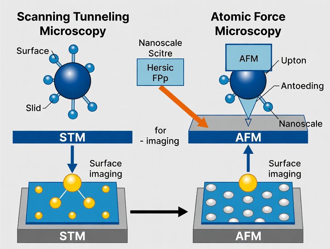
This article provides researchers, scientists, and drug development professionals with a comprehensive analysis of Scanning Tunneling Microscopy (STM) and Atomic Force Microscopy (AFM) for nanoscale imaging.
STM vs AFM: A Comparative Guide to Nanoscale Imaging for Biomedical Research
Abstract
This article provides researchers, scientists, and drug development professionals with a comprehensive analysis of Scanning Tunneling Microscopy (STM) and Atomic Force Microscopy (AFM) for nanoscale imaging. We explore the foundational principles, operational methodologies, and specific applications relevant to biological and materials science. The guide offers practical troubleshooting advice, optimization strategies, and a direct comparison of the two techniques to validate their suitability for various research scenarios. This serves as a critical resource for selecting the optimal tool for structural biology, nanoparticle characterization, and advanced biomaterial development.
Understanding the Core Principles: How STM and AFM Visualize the Nanoworld
Within the comparative research framework of Scanning Tunneling Microscopy (STM) versus Atomic Force Microscopy (AFM) for nanoscale imaging, the quantum tunneling effect is not merely a physical curiosity but the foundational operational principle of STM. This whitepaper elucidates the technical basis of this effect as it applies to STM, contrasting it with the force-based detection of AFM. STM's unique capability for atomic-resolution imaging and electronic spectroscopy stems directly from the quantum mechanical tunneling of electrons between a sharp metallic tip and a conductive sample.
Theoretical Foundation of Quantum Tunneling in STM
The quantum tunneling phenomenon occurs when electrons traverse a classically forbidden potential barrier, such as the vacuum gap between the STM tip and sample. The probability is governed by the time-independent Schrödinger equation. For a one-dimensional rectangular barrier of height φ (the work function, typically 4-5 eV) and width d (the tip-sample separation), the tunneling probability T is approximately: T ∝ exp(-2κd), where κ = √(2mφ)/ħ. This exponential dependence on distance is the origin of STM's exceptional vertical sensitivity (~0.01 nm).
A critical comparison between STM and AFM is summarized in Table 1.
Table 1: Core Operational Principle Comparison: STM vs. AFM
| Parameter | Scanning Tunneling Microscopy (STM) | Atomic Force Microscopy (AFM) |
|---|---|---|
| Fundamental Interaction | Quantum Tunneling Current | Interatomic Forces (Van der Waals, etc.) |
| Requirement | Electrically Conductive Sample | Conductivity not required; works on insulators |
| Primary Measured Quantity | Tunneling Current (pA to nA) | Force (via cantilever deflection, nN to pN) |
| Resolution (Lateral) | Atomic (~0.1 nm) | Near-atomic (~0.5 nm) |
| Resolution (Vertical) | ~0.01 nm | ~0.1 nm |
| Operational Modes | Constant Current, Constant Height | Contact, Tapping, Non-Contact |
| Sample Modification | Possible via high bias/current | Possible via mechanical force |
| Environment | Ultra-high vacuum to air, liquid | Ultra-high vacuum to air, liquid |
Experimental Protocols for STM Imaging
The following protocol details a standard methodology for atomic-resolution STM imaging in Ultra-High Vacuum (UHV) conditions.
Protocol: Atomic-Resolution STM Imaging of a Metal Surface (e.g., Au(111)) Objective: To obtain an atomically resolved topographic image of a single-crystal metal surface using the constant-current mode of STM.
Materials & Reagents:
- UHV-STM System: Chamber with base pressure < 1×10⁻¹⁰ mbar.
- Piezoelectric Scanner: Calibrated for x, y, z motion with sub-Ångström precision.
- Electrochemically Etched Tungsten or PtIr Tip: Clean, sharp tip prepared in situ.
- Single-Crystal Sample (e.g., Au(111)): Mounted on a sample holder.
- Sample Preparation Kit: For in vacuo cleaning via cycles of Ar⁺ sputtering (1-2 keV) and annealing (~700 K).
- Vibration Isolation System: Active or passive isolation table.
- Electronics: Bias voltage source, current preamplifier, feedback control loop.
Procedure:
- Sample Preparation: Introduce the Au(111) crystal into the UHV chamber. Perform multiple cycles of argon ion sputtering (15-20 minutes, 1 keV) followed by annealing at approximately 720 K for 10 minutes to remove contaminants and reconstruct the surface.
- Tip Preparation: In situ clean the metal tip by electron bombardment heating or field emission/sputtering against a clean electrode to remove oxide layers.
- System Cooldown & Stabilization: Allow the system to thermally stabilize for at least 1 hour. Engage the vibration isolation system.
- Tip Approach: Use a coarse motor to bring the tip within ~100 nm of the sample, then engage the automated coarse approach until a tunneling current setpoint (e.g., 1 nA) is detected at a low bias (e.g., 0.1 V).
- Imaging Parameter Selection:
- Set the sample bias voltage (Vbias) typically between ±10 mV to ±2 V, depending on desired electronic contrast.
- Set the constant current setpoint (Iset) typically between 0.1 nA and 2 nA.
- Set the feedback loop gain to ensure stable tracking without oscillation.
- Scan Acquisition: Initiate a raster scan over the desired area (e.g., 10 nm x 10 nm). The feedback loop continuously adjusts the tip height z to maintain Itunnel = Iset. The z(x,y) data is recorded as the topographic image.
- Data Processing: Post-process the raw data using plane leveling and optional low-pass filtering to remove thermal drift and noise.
Visualization of STM Operation and Comparison
Diagram 1: STM Constant Current Mode Feedback Loop
Diagram 2: STM vs AFM Core Physical Principles
The Scientist's Toolkit: Essential Research Reagent Solutions for STM
Table 2: Key Materials & Reagents for STM Research
| Item | Function/Description | Typical Specification/Example |
|---|---|---|
| Single-Crystal Substrates | Provides an atomically flat, well-defined surface for imaging or as a deposition substrate. | Au(111), Highly Oriented Pyrolytic Graphite (HOPG), Cu(111), Si(111)-7x7. |
| Tip Fabrication Materials | Source material for creating sharp, stable tunneling tips. | Tungsten (W) wire (0.25 mm dia.), Platinum-Iridium (Pt80Ir20) wire. |
| Electrolyte for Tip Etching | Used in electrochemical etching to produce sharp tip apices. | For W: 1-2M NaOH or KOH solution. For PtIr: Molten NaNO3 or CaCl2. |
| Calibration Gratings | Used for lateral and vertical calibration of the piezoelectric scanner. | 2D grating with known pitch (e.g., 100 nm ± 1 nm); step height standards. |
| Sputtering Gas | Inert gas used for in situ ion bombardment cleaning of sample and tip. | Research purity Argon (Ar, 99.9999%). |
| UHV-Compatible Sample Adhesives | For mounting samples and filaments. | High-purity tantalum foil, platinum clips, conductive epoxies (e.g., silver epoxy). |
| Molecular Deposition Sources | For depositing molecules or atoms onto clean surfaces for study. | Organic Molecular Beam Epitaxy (OMBE) crucibles, electron beam evaporators. |
Within the context of nanoscale imaging research, the choice between Scanning Tunneling Microscopy (STM) and Atomic Force Microscopy (AFM) is fundamental. STM relies on the quantum mechanical tunneling current between a sharp tip and a conductive sample, limiting it to conductive or semi-conductive surfaces. In contrast, AFM measures the local force between a tip and a sample surface, enabling imaging of virtually any material—conductive, insulating, or biological—in various environments. This universality makes AFM indispensable for fields like drug development, where imaging complex biomolecules in near-native conditions is critical. The core of this capability lies in the precise mechanical system of force sensing and deflection. This whitepaper provides an in-depth technical guide to this principle, which forms the mechanical heart of AFM.
Core Physical Principle: The Cantilever Spring
The AFM cantilever is a micro-fabricated beam that acts as a Hookean spring. Its deflection, ( z ), is directly proportional to the force, ( F ), applied at its tip via the spring constant, ( k ): [ F = -k \cdot z ] The sensitivity of force measurement is thus dictated by the spring constant (typically 0.01 - 100 N/m) and the precision with which deflection can be measured.
Table 1: Cantilever Properties and Applications
| Property | Typical Range | Relevance to Application |
|---|---|---|
| Spring Constant (k) | 0.01 - 100 N/m | Softer for biological samples, stiffer for hard materials. |
| Resonant Frequency | 1 kHz - 2 MHz | Higher for faster scanning in dynamic modes. |
| Tip Radius | < 10 nm (super-sharp) | Determines lateral resolution. |
| Material | Si, Si₃N₄, Si with Al coating | Affects reflectivity, stiffness, and biocompatibility. |
Deflection Detection Methods: Protocols and Implementation
The accurate measurement of sub-nanometer cantilever deflection is the central technical challenge. The following are detailed methodologies for the primary techniques.
Optical Beam Deflection (OBD) - Standard Protocol
Principle: A laser beam reflected off the cantilever onto a Position-Sensitive Photodetector (PSPD). Deflection changes the beam position on the PSPD.
Experimental Protocol:
- Alignment: Mount a cantilever with an appropriate k for the sample.
- Laser Positioning: Using micromanipulators, focus a diode laser (e.g., 670 nm) onto the cantilever's free end. Ensure a clean, round reflected spot.
- Photodetector Alignment: Direct the reflected beam to the center of a quadrant PSPD. Adjust so that the vertical (A+B)-(C+D) and lateral (A+C)-(B+D) differential signals are near zero at equilibrium.
- Calibration: Perform a force-curve on a rigid sample (e.g., sapphire). The known slope of the contact region (in volts) versus the piezo movement (in nm) yields the deflection sensitivity (nm/V).
- Spring Constant Calibration: Apply thermal tune method: measure the power spectral density of the cantilever's thermal fluctuations in air, fit to a Lorentzian, and derive k from the equipartition theorem: ( k = kB T / \langle z^2 \rangle ), where ( kB ) is Boltzmann's constant.
Piezoresistive Detection - Protocol
Principle: A piezoresistive material (doped Si) in the cantilever stem changes resistance under strain from deflection.
Experimental Protocol:
- Wheatstone Bridge: Integrate the piezoresistive cantilever as one arm of a Wheatstone bridge circuit.
- Balancing: With no applied force, adjust variable resistors in the bridge to null the output voltage.
- Measurement: Apply a constant bias voltage. Cantilever deflection unbalances the bridge, producing an output voltage proportional to strain.
- Calibration: Requires a separate displacement actuator to deflect the cantilever a known amount to establish V/nm sensitivity.
Interferometric Detection - Protocol
Principle: Measures the path difference between light reflected from the cantilever and a reference, providing absolute displacement.
Experimental Protocol:
- Setup: Use a fiber-optic or free-space Michelson interferometer. One mirror is replaced by the AFM cantilever.
- Laser Stabilization: Use a frequency-stabilized HeNe or diode laser to minimize phase noise.
- Quadrature Detection: Employ a setup generating two interference signals 90° out of phase to determine both magnitude and direction of displacement.
- Fringe Counting: Displacement is measured by counting the interference fringes; each fringe corresponds to a λ/2 displacement.
Table 2: Deflection Detection Method Comparison
| Method | Sensitivity | Bandwidth | Advantages | Disadvantages |
|---|---|---|---|---|
| Optical Beam Deflection | ~0.1 nm | ~10 MHz | Simple, high sensitivity, robust. | Requires reflective surface; sensitive to ambient light. |
| Piezoresistive | ~0.1 nm | ~1 MHz | Self-sensing, works in opaque fluids. | Lower sensitivity; generates heat. |
| Interferometric | ~0.01 nm | ~100 MHz | Highest absolute accuracy; direct. | Complex setup; sensitive to vibrations. |
Operational Modes: From Deflection to Image
The control system uses the deflection signal as feedback. The core modes are:
- Contact Mode: Deflection (force) is held constant via feedback. The error signal directly maps topography.
- Dynamic Mode (Oscillating): The cantilever is driven at or near resonance. Changes in amplitude, frequency, or phase due to tip-sample interactions are used as feedback. This includes AM-AFM (Amplitude Modulation) and FM-AFM (Frequency Modulation).
AFM Feedback Control Logic
The Scientist's Toolkit: Key Research Reagent Solutions
Table 3: Essential Materials for Biomolecular AFM Force Spectroscopy
| Item | Function & Rationale |
|---|---|
| Functionalized Cantilevers | Tips chemically modified with specific ligands (e.g., biotin, Ni-NTA, antibodies) to enable specific binding force measurements with target molecules. |
| PEG Crosslinkers | Polyethylene glycol spacers tether ligands to the tip/surface; provide flexibility, reduce non-specific adhesion, and define precise rupture length. |
| Mica Substrates (Muscovite) | Atomically flat, negatively charged surface ideal for adsorbing biomolecules (proteins, DNA) via divalent cations (e.g., Ni²⁺, Mg²⁺). |
| PBS Buffer (1x, pH 7.4) | Standard physiological buffer for maintaining protein stability and function during liquid-phase imaging/spectroscopy. |
| BSA or Casein | Used as blocking agents to passivate surfaces and cantilevers, minimizing non-specific protein adsorption. |
| Calibration Gratings (TGZ Series) | Samples with known pitch and height (e.g., 10 μm pitch, 180 nm depth) for verifying scanner and deflection sensitivity calibration. |
Advanced Force Spectroscopy: Unlocking Molecular Interactions
Beyond imaging, measuring deflection versus piezo extension yields a force-distance curve, the cornerstone of single-molecule force spectroscopy.
Single Molecule Force Curve Steps
Protocol for Receptor-Ligand Bond Strength Measurement:
- Functionalization: Cantilever tip is coated with a receptor protein via PEG crosslinker. Substrate is coated with the ligand.
- Approach: A single force curve is performed in relevant buffer. Thousands of curves are collected.
- Analysis: Curves showing specific unbinding events are identified by their characteristic rupture length (PEG spacer elongation). Rupture force is recorded.
- Statistics: A histogram of rupture forces is built. The most probable unbinding force is extracted. By varying the retraction speed, the kinetic off-rate (( k_{off} )) and energy landscape of the bond can be probed via Bell-Evans model.
While STM offers supreme atomic resolution on conductive surfaces, AFM's mechanical force-sensing core grants it unparalleled versatility. The precise measurement of cantilever deflection enables not only high-resolution topography of any material but also quantitative nanomechanical mapping and the dissection of inter- and intra-molecular forces at the single molecule level. For researchers and drug development professionals, this makes AFM an indispensable tool for characterizing nanomaterials, visualizing cellular structures, and measuring the binding forces critical to drug-target interactions, solidifying its role as a cornerstone of modern nanoscience.
This whitepaper provides an in-depth technical guide on the fundamental sample conductivity requirements for Scanning Tunneling Microscopy (STM) and Atomic Force Microscopy (AFM), two cornerstone techniques in nanoscale imaging. The choice between these methods is primarily dictated by the electrical properties of the sample, creating a critical divide in experimental design and application scope, particularly in materials science and biophysical research.
The Core Technical Divide: STM vs. AFM
Scanning Tunneling Microscopy (STM) operates on the principle of quantum tunneling. A sharp metallic tip is brought within angstroms of a conductive or semi-conductive sample surface. A bias voltage is applied, and the resulting tunneling current, which is exponentially dependent on the tip-sample separation, is measured to maintain a constant distance while raster-scanning. This provides topographic and electronic information at atomic resolution.
Atomic Force Microscopy (AFM) measures the interatomic forces (e.g., Van der Waals, mechanical contact) between a tip on a flexible cantilever and the sample surface. The deflection of the cantilever is monitored, allowing imaging of any solid surface—conductive or non-conductive—in various environments (air, liquid, vacuum). AFM modes include contact, non-contact, and tapping mode.
Key Quantitative Comparison
Table 1: Core Comparison of STM and AFM Based on Sample Conductivity Requirements
| Parameter | Scanning Tunneling Microscopy (STM) | Atomic Force Microscopy (AFM) |
|---|---|---|
| Sample Conductivity | Mandatory. Requires conductive or semiconductive samples. | Not Required. Can image conductive and insulating surfaces. |
| Primary Measurand | Tunneling Current (pA to nA) | Force (pN to nN) / Cantilever Deflection |
| Lateral Resolution | Atomic (~0.1 nm) | Sub-nanometer to several nm |
| Vertical Resolution | ~0.01 nm | ~0.1 nm |
| Imaging Environment | Typically UHV, liquid, or air | UHV, liquid, air, controlled gas |
| Sample Preparation | Often complex (clean, flat, conductive) | Generally simpler; can image native states. |
| Key Applications | Atomic surfaces, electronic structure, manipulation | Polymers, biological molecules, insulators, composites |
Experimental Protocols
Protocol 1: STM Imaging of a Conductive Surface (e.g., HOPG)
Objective: Achieve atomic-resolution imaging of Highly Oriented Pyrolytic Graphite (HOPG).
- Tip Preparation: Electrochemically etch a tungsten (W) or Pt-Ir wire to a sharp point. Clean via high-voltage pulses in situ.
- Sample Preparation: Cleave HOPG using adhesive tape to expose a fresh, atomically flat basal plane. Mount on a conductive sample holder.
- System Setup: Load tip and sample into UHV or controlled atmosphere chamber. Evacuate or purge to remove contaminants.
- Approach: Use coarse motors to bring tip within ~100 nm of the surface, then engage piezoelectric coarse approach until a tunneling current is detected (setpoint: 0.1-1 nA, bias: 10-100 mV).
- Imaging: Engage feedback loop. Scan in constant current mode. Parameters: Scan size 10x10 nm², scan rate 1-4 Hz, integral and proportional gains adjusted for stable feedback.
- Data Analysis: Apply plane subtraction and mild filtering to raw topographic data to visualize the hexagonal carbon lattice.
Protocol 2: AFM Imaging of a Non-Conductive Biological Sample (e.g., Protein on Mica)
Objective: Image the tertiary structure of adsorbed proteins in buffer solution.
- Cantilever Selection: Choose a silicon nitride cantilever for liquid imaging (typical spring constant ~0.1 N/m, resonant frequency ~10 kHz in liquid).
- Substrate Preparation: Cleave a fresh mica disk. Treat with divalent cation solution (e.g., 10 mM NiCl₂) to promote protein adhesion.
- Sample Deposition: Incubate 10-50 µL of dilute protein solution (e.g., 10 µg/mL) on mica for 2-5 minutes. Rinse gently with appropriate buffer to remove unbound molecules.
- Liquid Cell Assembly: Mount the sample in the fluid cell. Inject imaging buffer to fully submerge the sample and the mounted cantilever.
- Engagement & Imaging: Use optical lever system to align laser on cantilever back. Approach surface in tapping (AC) mode. Set drive frequency slightly below resonance. Optimize drive amplitude and setpoint to achieve stable, minimal-force imaging.
- Data Analysis: Measure particle heights from cross-sectional analysis to determine protein dimensions, avoiding lateral measurements due to tip convolution.
Logical Workflow for Technique Selection
Title: Decision Workflow: STM vs AFM Selection
The Scientist's Toolkit: Key Research Reagent Solutions
Table 2: Essential Materials and Reagents for STM and AFM Experiments
| Item | Function | Typical Application/Example |
|---|---|---|
| Conductive Substrates | Provides a flat, electrically conducting base for sample deposition for STM or conductive AFM. | HOPG, Au(111) on mica, highly doped silicon wafers. |
| Atomically Flat Insulating Substrates | Provides an ultra-flat, inert surface for adsorbing non-conductive samples, especially for AFM. | Muscovite mica, sapphire (Al₂O₃), cleaved alkali halides (e.g., KCl). |
| Conductive AFM Probes | Silicon probes coated with a conductive layer (Pt/Ir, doped diamond) to measure current or potential. | Piezoresistive conductivity mapping, Scanning Kelvin Probe Force Microscopy (SKPFM). |
| Sharp Metallic STM Tips | Acts as the scanning electrode; sharpness and cleanliness are critical for high resolution. | Electrically etched Tungsten (W) wire, mechanically cut Pt-Ir alloy wire. |
| Cantilevers for Liquid/AFM | Low spring constant levers with reflective coating for operation in fluid environments. | Silicon nitride cantilevers (e.g., DNP-S from Bruker) for bio-AFM in buffer. |
| Sample Mounting Adhesives | Secures sample to holder without interfering with measurement (e.g., conductive for STM). | Conductive epoxy (for STM), double-sided tape, quick-drying cyanoacrylate. |
| Calibration Gratings | Standard samples with known pitch and height for verifying AFM scanner calibration. | TGZ1-3D (periodic pillars), HS-100MG (height standards) from NT-MDT or Bruker. |
| Surface Functionalization Kits | Chemicals to modify substrate surface properties to promote specific sample adhesion. | Aminosilanes (e.g., APTES) for covalent bonding, poly-L-lysine for electrostatic adsorption of cells/DNA. |
Advanced Modalities Bridging the Divide
Recent advancements have created hybrid or specialized modes that blur the conductivity divide:
- Conductive AFM (C-AFM): Uses a conductive tip to map local conductivity and topography of non-uniform samples.
- Electrochemical AFM (EC-AFM): Allows AFM imaging within an electrochemical cell to study in situ processes like corrosion or battery cycling.
- Scanning Tunneling Spectroscopy (STS): An STM-based technique to measure the local density of electronic states, requiring conductive samples.
Title: Application Pathways from Core Sample Property
The conductivity requirement forms the most fundamental fork in the road for selecting a nanoscale imaging technique. STM offers unparalleled electronic and atomic resolution but is restricted to conductive samples. AFM, with its versatility in imaging any solid surface and operating in diverse environments, is the indispensable tool for non-conductive and soft matter, including most biological systems. The choice is not merely technical but defines the possible questions a researcher can ask, making an understanding of this divide critical for experimental design in nanotechnology and drug development, where characterizing both conductive nanomaterials and insulating biomolecules is paramount.
This technical guide examines the core data outputs of Scanning Tunneling Microscopy (STM) and Atomic Force Microscopy (AFM) within nanoscale imaging research. The central thesis posits that while both are premier scanning probe techniques, their inherent physical principles dictate fundamentally different data types and analytical capabilities. STM provides unparalleled electronic structure information, whereas AFM excels in quantifying nanomechanical and multifunctional properties, a distinction critical for fields like drug development where surface chemistry and biomechanics are paramount.
Core Principles and Inherent Data Outputs
Scanning Tunneling Microscopy (STM)
STM operates based on quantum tunneling. A sharp metallic tip is brought within ~1 nm of a conductive sample, and a bias voltage is applied. The resulting tunneling current, exponentially dependent on the tip-sample separation, is used to maintain a constant distance while rastering, generating topographical maps.
Primary Inherent Data Outputs:
- Topography (z(x,y)): Atomic-scale real-space contour of the surface.
- Tunneling Current (I(x,y)): A direct map at constant height, sensitive to local electronic density of states (LDOS).
- Scanning Tunneling Spectroscopy (STS) Data: I-V or dI/dV-V spectra acquired at fixed points, quantifying local electronic structure (e.g., band gaps, molecular orbitals).
Atomic Force Microscopy (AFM)
AFM measures forces between a nanoscopic tip on a cantilever and the sample surface. Deflection of the cantilever, monitored by a laser spot, is used for feedback. Its operation is not limited to conductive samples.
Primary Inherent Data Outputs:
- Topography (z(x,y)): Nanoscale to atomic-scale height data.
- Tip-Sample Interaction Force: The raw signal, from which multiple derivatives are extracted.
- Phase Signal: In dynamic modes, the lag between cantilever drive and oscillation, sensitive to energy dissipation (viscoelasticity, adhesion).
- Frequency Shift / Dissipation: In non-contact modes, key outputs for quantifying long-range forces and stiffness.
- Cantilever Deflection / Bending: Direct measure of applied normal force or adhesion hysteresis.
The following table summarizes the inherent data outputs and their primary applications.
Table 1: Inherent Data Outputs of STM vs. AFM
| Technique | Core Data Output | Physical Origin | Primary Information Conveyed | Typical Resolution |
|---|---|---|---|---|
| STM | Topography (Constant Current) | Feedback-maintained tip height | Surface atom corrugation | 0.1 nm lateral, 0.01 nm vertical |
| Tunneling Current Map | Quantum tunneling probability | Spatial variation of LDOS | ~1 nm electronic | |
| dI/dV Spectroscopy | Differential conductance | Local electronic density of states | Band structure, molecular orbitals, defects | Energy resolution: <1 meV |
| AFM | Topography (Constant ∆f/F) | Feedback-maintained tip height | Surface morphology | 1-5 nm lateral, 0.1 nm vertical |
| Force-Distance Curve | Cantilever deflection vs. Z-piezo | Integrated tip-sample force vs. gap | Adhesion, elasticity, charge, hydration forces | Force resolution: ~1 pN |
| Phase Image | Oscillation phase lag | Energy dissipation per cycle | Viscoelasticity, composition, adhesion hysteresis | ~5 nm compositional |
| Frequency Shift (∆f) | Resonant frequency shift | Gradient of tip-sample force | Stiffness, long-range forces | ~10 pN/√Hz force gradient |
| Peak Force Tapping Data | Maximum force per tap | Direct force control | Nanomechanics (Modulus, Adhesion, Deformation) | <5 nm lateral, ~10 pN force |
Experimental Protocols for Key Measurements
Protocol 1: STS for Molecular Orbital Imaging (STM)
Objective: To map the spatial distribution of a specific molecular orbital on a conductive surface.
- Sample Prep: Sublimate target molecule (e.g., pentacene) onto an ultra-clean, atomically flat conductive substrate (Au(111) or Ag(111)) in UHV.
- STM Stabilization: Cool system to 4.2 K or 77 K to reduce thermal drift. Approach tip and obtain stable topography in constant-current mode.
- Spectroscopy Point Selection: Identify a target molecule from topography.
- Feedback Disable & Positioning: Disable feedback loop and position tip over desired (x,y) coordinate.
- Bias Ramp & Data Acquisition: Ramp the sample bias voltage (e.g., -2V to +2V) while measuring tunneling current (I). Use lock-in amplifier with a small AC modulation (e.g., 10 mV, 1 kHz) superimposed on the DC bias to simultaneously acquire dI/dV.
- Grid Acquisition: Perform step 5 over a defined (x,y) grid.
- Data Processing: Plot dI/dV spectra for specific points. Generate constant-height dI/dV maps by plotting the dI/dV signal at a specific bias voltage for each pixel in the grid.
Protocol 2: Peak Force Tapping Nanomechanical Mapping (AFM)
Objective: To simultaneously acquire topography and quantitative nanomechanical properties (elastic modulus, adhesion) in ambient or fluid conditions.
- Cantilever & Probe Selection: Use a cantilever with a calibrated spring constant (k ~ 0.1-5 N/m) and a sharp tip (radius <10 nm). Select appropriate resonant frequency (f0 ~ 10-150 kHz).
- System Setup: Engage in standard tapping mode to locate area of interest. Switch to Peak Force Tapping mode.
- Parameter Optimization: Set the peak force setpoint (typically 10-500 pN) to minimize sample deformation. Adjust the oscillation amplitude (~50-150 nm) and frequency (~0.5-2 kHz, far below f0).
- Capture & Processing: Enable capture of the full force-distance curve at each pixel (~1-10 kHz curve rate). Use a real-time processing model (e.g., DMT, Sneddon) to fit the retraction curve and derive reduced Young's modulus and adhesion force.
- Mapping: Raster the tip while maintaining the peak force setpoint. Topography is derived from the piezo height at the peak force point. Modulus and adhesion maps are generated from the fitted parameters per pixel.
Visualizing Workflows and Data Relationships
STM Operational Modes and Derived Data Outputs
AFM Signal Hierarchy and Multifunctional Outputs
The Scientist's Toolkit: Research Reagent Solutions & Materials
Table 2: Essential Materials for STM and AFM Nanoscale Research
| Item | Function | Typical Specification/Example |
|---|---|---|
| STM Specific | ||
| UHV-STM System | Provides vibration isolation and atomically clean environment for electronic measurements. | Base pressure < 1×10⁻¹⁰ mbar, cryogenic capability (4K). |
| Conductive Substrates | Atomically flat, clean surface for adsorption of molecules/atoms. | Au(111) on mica, HOPG, cleaved NbSe₂, Si(111)-7×7. |
| Molecular Beam Epitaxy (MBE) Source | For precise thermal evaporation of organic molecules or metals in UHV. | Knudsen cell with temperature controller. |
| AFM Specific | ||
| Functionalized AFM Tips | Modify tip chemistry to measure specific interactions (e.g., ligand-receptor). | Silicon nitride tips with -COOH, -NH₂, or PEG-biotin coatings. |
| Calibration Standards | For verifying lateral and vertical scale, and quantifying tip radius/spring constant. | TGZ1/TGQ1 gratings, PS/LDPE blend, Bruker PFQNM-LC-Al. |
| Liquid Cell | For imaging in physiological buffers or organic solvents. | Closed or flow-through cell with O-rings. |
| Common | ||
| Vibration Isolation Table | Isolates instrument from building and acoustic vibrations. | Active or passive isolator with >90% efficiency above 5 Hz. |
| Acoustic Enclosure | Minimizes airborne noise interference, critical for high-resolution AFM. | Custom or manufacturer-provided hood. |
| Anti-vibration Gloves | Prevents thermal drift and disturbances during sample/tip handling. | Nitrile gloves, often worn over temperature-stabilizing inner gloves. |
STM and AFM are complementary pillars of nanoscale characterization. STM's inherent output is electron-tunneling probability, making it a unique tool for solid-state physics and molecular electronics, directly revealing electronic structure beyond topography. AFM's inherent output is force, making it a versatile, materials-agnostic tool that derives a beyond topography suite of nanomechanical, chemical, and functional property maps. The choice for drug development research hinges on the question: is electronic orbital structure (STM) or nanomechanical/chemical interaction (AFM) more critical for the system under investigation? Increasingly, correlative use of both techniques provides the most comprehensive nanoscale portrait.
Operational Modes and Biomedical Applications: From Setup to Discovery
Scanning Tunneling Microscopy (STM) remains a cornerstone of nanoscale surface science, offering atomic-resolution imaging unmatched by many other techniques. Within a broader thesis comparing STM and Atomic Force Microscopy (AFM) for nanoscale research, the choice of operational mode is a fundamental differentiator. While AFM measures forces, STM relies on quantum tunneling current. This guide details the two primary STM imaging modes—Constant Current and Constant Height—contrasting their principles, applications, and experimental protocols. This comparison is critical for researchers, particularly in fields like drug development, where visualizing molecular adsorption, semiconductor defects, or catalyst surfaces informs material design and function.
Fundamental Principles & Comparative Analysis
Constant Current Mode (CCM): A feedback loop continuously adjusts the tip height (z-piezo voltage) to maintain a pre-set tunneling current (It) as the tip scans (x,y). The recorded z-displacement maps the surface topography. Constant Height Mode (CHM): The tip height is fixed, and variations in the tunneling current are recorded as the tip scans. This enables faster scanning but requires atomically flat surfaces.
A quantitative comparison of the core characteristics is summarized below.
Table 1: Comparative Analysis of STM Operational Modes
| Parameter | Constant Current Mode (CCM) | Constant Height Mode (CHM) |
|---|---|---|
| Controlled Variable | Tunneling Current (It) | Tip-Sample Separation (z) |
| Measured Variable | Tip Height (z-piezo voltage) | Tunneling Current (It) |
| Feedback Loop | Active (on) | Inactive (off) or very high gain |
| Typical Scan Speed | Slow (0.1 - 10 Hz) | Fast (10 - 200+ Hz) |
| Topographic Accuracy | High (prevents crash) | Low (risk of tip crash) |
| Surface Requirement | Tolerates moderate roughness | Requires atomically flat surfaces |
| Ideal Application | Rough surfaces, atomic corrugation, spectroscopy | Fast imaging, diffusion dynamics, electronic structure mapping |
| Lateral Resolution | Atomic | Atomic (potentially higher due to speed) |
| Primary Risk | Feedback oscillation, slow speed | Tip or sample damage |
Experimental Protocols
Protocol for Constant Current Mode Imaging
- Sample & Tip Preparation: Prepare a clean, conductive sample (e.g., cleaved HOPG, annealed metal single crystal). Etch a sharp metal tip (e.g., Pt/Ir or W).
- System Setup: Load sample and tip into ultra-high vacuum (UHV) or controlled environment. Achieve base pressure (<1×10⁻¹⁰ mbar for UHV).
- Approach: Use a coarse approach mechanism to bring the tip within ~1 mm of the sample. Engage the fine piezoelectric approach until a tunneling current is detected (typical setpoint: 0.1 - 2 nA, bias: 10 - 1000 mV).
- Feedback Parameter Tuning: Set the feedback loop gains (P, I). Use an oscilloscope to optimize for critical damping—sufficient gain for tracking topography without oscillation.
- Image Acquisition: Select scan area (typically 2 nm x 2 nm to 1 μm x 1 μm). Initiate scan. The computer records the z-piezo voltage at each (x,y) point, converting it to a topographic image.
- Post-Processing: Apply plane subtraction and line-leveling routines to correct for sample tilt and thermal drift.
Protocol for Constant Height Mode Imaging
- Prerequisite - Surface Flattening: First, image a large area in Constant Current Mode to locate an atomically flat terrace.
- Setpoint Stabilization: On the flat terrace, stabilize the tip at the desired tunneling current and bias.
- Feedback Disengagement: Switch the feedback loop to "off" or set the gain to a minimal value. The z-piezo voltage is now fixed.
- High-Speed Scan: Initiate a fast raster scan. The analog-to-digital converter records the instantaneous tunneling current at each pixel.
- Current Signal Mapping: The recorded current map, I(x,y), is displayed. Brighter areas correspond to higher current (lower effective barrier or closer proximity).
- Vigilance: Monitor the current trace continuously. Abort the scan immediately if the current exceeds a safe threshold to prevent tip crash.
Visualization: Operational Workflow & Decision Logic
STM Mode Selection Logic
The Scientist's Toolkit: Essential Research Reagents & Materials
Table 2: Key Research Reagent Solutions for STM Experiments
| Item | Function | Typical Specification/Example |
|---|---|---|
| Conductive Substrates | Provides atomically flat, clean surface for adsorption or growth. | Highly Oriented Pyrolytic Graphite (HOPG), Au(111) on mica, single crystal silicon wafers. |
| Electrochemical Etching Solutions | For preparing sharp, reproducible metal tips. | W tip: 1-3M NaOH or KOH solution.Pt/Ir tip: Molten CaCl₂/NaCl mixture or electrochemical etching in CaCl₂/H₂O/C₂H₅OH. |
| Ultrasonic Cleaning Solvents | For degreasing tips and sample holders. | Sequential baths in acetone, isopropanol, and ethanol (semiconductor grade). |
| Sputtering/Ion Etch Gas | For in-situ sample and tip cleaning in UHV. | Research-grade Argon (Ar⁺) gas for bombardment. |
| Molecular Deposition Sources | For controlled dosing of adsorbates onto the substrate. | Knudsen Cell evaporators for organics, e-gas dosers for CO, H₂, O₂. |
| Vibration Isolation Fluid | Dampens acoustic and building vibrations. | Fluorinert or similar low-viscosity, dielectric fluid for damping tables. |
| Calibration Grids | Lateral and vertical calibration of the piezoelectric scanner. | 2D gratings (e.g., 180 nm pitch) and step height standards (e.g., 20 nm TiO₂). |
Atomic Force Microscopy (AFM) emerged from the foundational principles of Scanning Tunneling Microscopy (STM). While STM revolutionized nanoscale imaging by measuring quantum tunneling current between a sharp tip and a conductive sample, its fundamental limitation is the requirement for sample conductivity. AFM overcomes this by measuring intermolecular forces, enabling the study of insulating biological materials, polymers, and soft matter. This versatility is paramount for researchers in drug development and life sciences, where samples are often delicate, non-conductive, and require interrogation in near-native, often fluid, environments. The core of AFM's adaptability lies in its three primary operational modes—Contact, Tapping, and Non-Contact—each offering a distinct balance of force, resolution, and sample preservation.
Core Operational Modes: Principles and Applications
The choice of AFM mode is dictated by the sample's mechanical properties, adhesion, and required resolution. The fundamental difference lies in the tip-sample interaction regime.
Figure 1: Decision workflow for selecting an AFM mode for delicate samples.
Contact Mode
The tip remains in constant physical contact with the sample surface. The cantilever deflection, proportional to the normal force (Hooke's Law: F = -kz), is kept constant via feedback. Lateral forces (friction) are significant.
- Key Application: Imaging robust, well-immobilized samples in liquid (e.g., supported lipid bilayers, live cell morphology under physiological buffer).
- Protocol for Live Cell Imaging in Contact Mode:
- Sample Prep: Seed cells on a sterile, plasma-treated glass-bottom Petri dish. Allow adhesion for 24h.
- AFM Setup: Mount dish on scanner stage. Use a silicon nitride (Si₃N₄) cantilever (spring constant ~0.01-0.1 N/m).
- Fluid Cell Engagement: Assemble fluid cell, fill with pre-warmed CO₂-independent culture medium.
- Laser Alignment: Align laser on cantilever back, adjust photodiode for sum and difference zero.
- Approach & Engagement: Use automated approach to bring tip into contact with the substrate near a cell.
- Parameter Set: Setpoint force: 0.5-2 nN. Integral and proportional gains optimized to minimize oscillation. Scan rate: 0.5-1 Hz.
- Imaging: Acquire 256x256 pixel topographic and deflection images.
Tapping Mode (Intermittent Contact)
The cantilever is oscillated at or near its resonant frequency (tens to hundreds of kHz). The amplitude of oscillation is damped by intermittent tip-sample contact and used as the feedback signal. Lateral forces are minimized.
- Key Application: The workhorse for delicate, adhesive, or loosely bound samples in air or fluid (e.g., proteins, DNA, polymers, mammalian cells).
- Protocol for Amyloid Fibril Imaging in Air (Tapping Mode):
- Sample Prep: Deposit 10 µL of fibril suspension (e.g., α-synuclein) onto freshly cleaved mica for 2 min. Rinse with ultrapure water and dry under gentle nitrogen stream.
- AFM Setup: Mount mica disk on magnetic stub. Use a doped silicon cantilever (resonant frequency ~300 kHz, spring constant ~40 N/m).
- Tune Resonance: Autotune to find the first resonant peak. Set drive frequency to this value.
- Approach: Engage with a free-air amplitude (A₀) of ~1.0 V and a setpoint amplitude (A_sp) ratio of ~0.8-0.9.
- Parameter Set: Optimize feedback gains to track features without ringing. Scan rate: 0.8-1.5 Hz.
- Imaging: Acquire height and phase images simultaneously. Phase signal reveals material stiffness variations.
Non-Contact Mode
The tip oscillates just above the sample surface (1-10 nm) without making contact. Attractive van der Waals forces cause a slight decrease in oscillation frequency (or amplitude). This frequency shift is the feedback signal.
- Key Application: Achieving atomic-scale resolution on clean, atomically flat surfaces in ultra-high vacuum (UHV) or controlled environments. Less common for biological samples due to capillary forces in air.
- Protocol for Atomically-Resolved Imaging of Mica in UHV:
- Sample Prep: Cleave muscovite mica in a glovebox attached to the UHV load-lock. Transfer to UHV chamber (pressure <1x10⁻¹⁰ mbar).
- AFM Setup: Use a qPlus sensor (stiff tuning fork with a tungsten tip) or a very stiff Si cantilever. Cool the stage to 4.2 K (liquid helium) to minimize thermal drift.
- Frequency Modulation (FM) Detection: Oscillate tip with constant amplitude (~0.5 Å). Use a phase-locked loop (PLL) to track the resonant frequency shift (Δf).
- Parameter Set: Set Δf setpoint to a negative value (e.g., -5 to -50 Hz) corresponding to the attractive regime. Use low scan rates (several minutes per line).
- Imaging: Acquire constant Δf topography, revealing the hexagonal lattice of surface atoms or adsorbed molecules.
Quantitative Comparison of AFM Modes
Table 1: Operational Parameters and Performance Metrics for Core AFM Modes
| Parameter | Contact Mode | Tapping Mode | Non-Contact Mode (FM-AFM) |
|---|---|---|---|
| Tip-Sample Force | High (nN to µN) | Low (pN to nN) | Very Low (pN) |
| Force Type | Repulsive (Constant) | Intermittent Repulsive | Attractive (Van der Waals) |
| Lateral Shear | High | Very Low | Negligible |
| Typical Environment | Liquid, Air, Controlled Gas | Air, Liquid (most common) | UHV, Low-Temperature |
| Best Resolution | ~0.5 nm (liquid) | ~1 nm (air), ~0.5 nm (liquid) | Atomic (<0.1 nm) |
| Sample Damage Risk | High (for soft samples) | Low | Minimal |
| Primary Feedback Signal | Cantilever Deflection | Oscillation Amplitude Damping | Resonant Frequency Shift (Δf) |
| Key Cantilever Property | Low Spring Constant (k ~ 0.01-0.5 N/m) | High Resonant Frequency, Q-factor | Very High Stiffness (k > 1000 N/m), High Q |
Table 2: Suitability for Delicate Sample Types in Research
| Sample Type | Recommended Mode(s) | Critical Consideration | Key Reagent/Material |
|---|---|---|---|
| Live Mammalian Cells | Contact (Liquid), Tapping (Liquid) | Force setpoint < 1 nN; CO₂ & temp control | CO₂-Independent Medium, Si₃N₄ Cantilevers |
| Isolated Proteins / DNA | Tapping (Air/Liquid) | Avoid dehydration artifacts; soft cantilevers in fluid | Freshly Cleaved Mica, APS-coated Mica |
| Lipid Bilayers | Contact (Liquid) | Sub-micron scan size; low force | Supported Lipid Bilayer on Mica/Silica |
| Polymers / Hydrogels | Tapping (Air/Liquid) | Phase imaging for material contrast | - |
| 2D Materials (e.g., Graphene) | Non-Contact (UHV), Tapping (Air) | Cleanliness is paramount | Highly Oriented Pyrolytic Graphite (HOPG) |
The Scientist's Toolkit: Essential Research Reagent Solutions
Table 3: Key Materials and Reagents for AFM of Delicate Samples
| Item | Function & Rationale |
|---|---|
| Freshly Cleaved Mica (Muscovite) | Provides an atomically flat, negatively charged, hydrophilic substrate for adsorbing biomolecules (proteins, DNA) via electrostatic interactions. |
| Aminopropylsilatrane (APS)-treated Mica | Functionalizes mica with a positive amine charge, enabling strong immobilization of negatively charged samples like DNA or certain proteins. |
| Silicon Nitride (Si₃N₄) Cantilevers (V-shaped) | Low spring constant (soft) probes essential for contact mode imaging in liquid to minimize damage to live cells and soft tissues. |
| Doped Silicon Cantilevers (Rectangular) | Stiffer probes with high resonant frequency and reflective coating, optimized for high-resolution Tapping Mode in air and liquid. |
| qPlus Sensors (for NC-AFM) | Quartz tuning fork-based force sensors with ultra-high stiffness and stability, enabling true atomic resolution in UHV. |
| CO₂-Independent Cell Culture Medium | Maintains pH without a controlled atmosphere during AFM imaging sessions inside the fluid cell, preserving cell viability. |
| Poly-L-Lysine or Cell-Tak | Adhesive coatings used to immobilize cells or tissue sections more firmly to substrates, reducing detachment during scanning. |
| Calibration Gratings (e.g., TGZ series) | Samples with known pitch and step height (e.g., 10 µm pitch, 180 nm depth) for lateral and vertical calibration of the AFM scanner. |
The choice between Scanning Tunneling Microscopy (STM) and Atomic Force Microscopy (AFM) for nanoscale biological imaging is fundamentally dictated by the sample's conductivity and the required measurement environment. STM relies on a measurable tunneling current between a conductive tip and a conductive sample, limiting its application to electrically conductive or thinly coated substrates in vacuum or air. In contrast, AFM measures van der Waals forces between a tip and the surface, allowing it to image non-conductive biological samples in near-physiological conditions (liquid, air, or vacuum). This makes AFM the unequivocal technique for high-resolution, three-dimensional topographical imaging of soft, insulating biomolecules like viruses, proteins, and DNA, which is the focus of this technical guide.
Key Technical Principles of Biomolecular AFM
Imaging Modes for Biological Samples
- Contact Mode: The tip scans in constant contact with the sample surface. While it provides high resolution, the lateral forces can distort or displace soft biological specimens.
- Intermittent Contact (Tapping) Mode: The tip oscillates at its resonant frequency, intermittently touching the surface. This is the predominant mode for biomolecular imaging as it minimizes lateral forces and sample damage.
- Non-Contact Mode: The tip oscillates above the sample surface without touching it. It offers the lowest force interaction but is challenging in liquids and typically provides lower resolution on biomolecules.
Environmental Control
Imaging in liquid is critical for maintaining native conformations. A fluid cell is used, allowing buffer exchange and temperature control. This enables real-time observation of dynamic processes.
Experimental Protocols for High-Resolution Biomolecular AFM
Protocol 1: Substrate Preparation for DNA and Protein Imaging
- Cleaning: Immerse freshly cleaved muscovite mica (V-1 grade) in a solution of 3-aminopropyltriethoxysilane (APTES) (0.01% v/v in Milli-Q water) for 20 minutes.
- Rinsing: Rinse the mica thoroughly with Milli-Q water to remove unbound silane and dry under a gentle stream of argon or nitrogen.
- Functionalization: The APTES-coated mica presents a positively charged surface, which electrostatically immobilizes negatively charged biomolecules like DNA or many proteins. For alternative functionalization, divalent cations (e.g., 10 mM MgCl₂ or NiCl₂) can be added to the deposition buffer to bridge negatively charged mica and molecules.
Protocol 2: Sample Deposition and Immobilization
- Deposition: Apply 10-50 µL of the biomolecule solution (e.g., 0.5-5 µg/mL for plasmid DNA, 10-50 nM for globular proteins) onto the prepared substrate.
- Incubation: Allow adsorption for 2-10 minutes, depending on concentration and affinity.
- Rinsing: Gently rinse with 1-2 mL of the appropriate imaging buffer (e.g., 10 mM HEPES, 10 mM MgCl₂, pH 7.5 for DNA) to remove loosely bound material.
- Loading: Immediately place the substrate into the AFM liquid cell, ensuring no air bubbles are trapped.
Protocol 3: AFM Imaging in Liquid
- Cantilever Selection: Use a sharp, nitride-coated silicon cantilever with a nominal spring constant of ~0.1-0.5 N/m and a resonant frequency of ~10-30 kHz in liquid.
- Engagement: Carefully engage the tip onto the substrate surface in liquid using the automated engagement routine.
- Parameter Optimization: Set the drive amplitude to achieve a free oscillation amplitude of 1-2 V. Set the setpoint amplitude to 85-95% of the free amplitude for stable, low-force imaging.
- Scanning: Initiate scanning with a slow scan rate (1-2 Hz) and 512-1024 samples per line to maximize resolution.
Table 1: AFM Imaging Performance for Key Biomolecules
| Biomolecule Class | Typical Sample Prep | Optimal Imaging Mode | Achievable Resolution (Height) | Lateral Resolution | Key Measurable Parameters |
|---|---|---|---|---|---|
| dsDNA (Plasmid) | APTES-mica or Mg²⁺/mica | Tapping in liquid | 0.2-0.3 nm | 1-2 nm | Contour length, persistence length, supercoiling density, protein-binding sites. |
| Proteins (Globular, e.g., BSA) | APTES-mica or hydrophobic surface | Tapping in liquid | 0.3-0.5 nm | 2-5 nm | Molecular volume, oligomeric state, conformational changes upon ligand binding. |
| Membrane Proteins (in lipid bilayer) | Supported lipid bilayer on mica | Tapping in liquid | 0.4-0.6 nm | 1-3 nm | 2D crystal lattice parameters, protein protrusion from bilayer, pore diameter. |
| Viruses (e.g., Adenovirus) | Poly-L-lysine coated mica | Tapping in liquid or air | 0.5-1.0 nm | 5-15 nm | Capsid dimensions (icosahedral symmetry), mechanical properties via nanoindentation. |
Table 2: Comparative Analysis: STM vs. AFM for Biomolecular Imaging
| Parameter | Atomic Force Microscopy (AFM) | Scanning Tunneling Microscopy (STM) |
|---|---|---|
| Imaging Principle | Mechanical force (van der Waals) | Quantum tunneling current |
| Sample Conductivity Requirement | Not required (works on insulators) | Mandatory (conductive or thin film on conductor) |
| Imaging Environment | Air, vacuum, liquid (physiological buffers) | Primarily ultra-high vacuum (UHV), some air |
| Typical Resolution (Biological Samples) | Sub-nanometer vertical; 1-5 nm lateral | Atomic on conductors; biomolecules require conductive coating, degrading resolution |
| Sample Preparation Complexity | Moderate (immobilization on substrate) | High (requires conductive coating or substrate) |
| Ability to Measure Mechanical Properties | Yes (nanoindentation, force spectroscopy) | No |
| Suitability for Dynamic Studies in Liquid | Excellent | Poor to None |
The Scientist's Toolkit: Research Reagent Solutions
| Item | Function in AFM Biomolecular Imaging |
|---|---|
| Muscovite Mica (V-1 Grade) | Atomically flat, negatively charged, cleavable substrate for sample adsorption. |
| 3-Aminopropyltriethoxysilane (APTES) | Silane used to functionalize mica with amine groups, creating a positively charged surface for nucleic acid/protein binding. |
| Poly-L-lysine | A polycationic polymer coated on mica to enhance adsorption of negatively charged samples like viruses or cells. |
| HEPES Buffer (10-50 mM, pH 7.0-7.5) | Standard biological imaging buffer with good buffering capacity in the physiological range, minimal salt crystallization. |
| MgCl₂ or NiCl₂ (1-20 mM) | Divalent cations that act as bridges to enhance adsorption of negatively charged biomolecules to bare mica. |
| Nitride-Coated Silicon Cantilevers (e.g., SNL, DNP-S) | Sharp, reflective tips with moderate spring constants optimized for tapping mode imaging in liquid. |
| Liquid Cell (Sealed or Flow-through) | Holds the sample and buffer, integrates with the scanner, and allows for in-situ experimentation. |
| Cleanroom Wipes & Compressed Air/Dust-Off | Essential for dust-free cleaning of stages, substrates, and liquid cell components to reduce artifacts. |
Visualization of Experimental Workflow and Analysis
AFM Biomolecular Imaging Workflow
Decision Logic: STM vs AFM for Biomolecules
Within the broader thesis comparing Scanning Tunneling Microscopy (STM) and Atomic Force Microscopy (AFM) for nanoscale imaging research, STM occupies a unique niche defined by its fundamental operational principle: quantum mechanical tunneling. Unlike AFM, which measures forces (e.g., van der Waals, mechanical contact) between a tip and a sample, STM requires a conductive or semiconductive sample to measure the tunneling current. This makes STM the unparalleled tool for mapping electronic structure—the local density of states (LDOS)—at atomic and molecular scales. While AFM excels in topographical imaging of insulating biological and soft materials in various environments, STM's capability to correlate topographic and electronic information is critical for research on conductive biomaterials (e.g., amyloid fibrils, cytochromes, bacterial nanowires) and engineered 2D substrates (e.g., graphene, transition metal dichalcogenides (TMDCs), MXenes). This guide details the application of STM for these material classes, focusing on protocols and quantitative insights.
Core Principles of STM for Electronic Structure
STM operates by bringing a sharp metallic tip within a few angstroms of a conductive sample. A bias voltage (Vbias) applied between them allows electrons to tunnel through the vacuum barrier. The resulting current (It) is exponentially dependent on the tip-sample separation (d): It ∝ Vbias ρs(r, EF) exp(-2κd) where κ is the decay constant and ρs is the sample LDOS at the Fermi level (EF). By scanning the tip and regulating either current (constant-current mode) or height (constant-height mode), one obtains a map. Spectroscopy modes—I vs. V (I-V) or dI/dV vs. V—directly probe the electronic density of states as a function of energy at a fixed location.
Application to Conductive Biomaterials
Certain biomaterials exhibit sufficient conductivity for STM investigation, often via electron hopping mechanisms or metallic co-factors.
Key Conductive Biomaterial Systems
- Amyloid Fibrils: Some demonstrate metallic-like conductivity under specific conditions.
- Bacterial Nanowires (e.g., Geobacter sulfurreducens pilin): Exhibit long-range electron transport.
- Redox Proteins (e.g., Cytochrome c): Heme groups facilitate electron tunneling.
- DNA-based Structures: Charge transport along π-stacked bases in dry, ordered films.
Experimental Protocol: STM of Cytochrome c on HOPG
Objective: To image and perform spectroscopy on cytochrome c molecules adsorbed on Highly Oriented Pyrolytic Graphite (HOPG) to locate the heme group electronically.
Methodology:
- Substrate Preparation: HOPG is freshly cleaved using adhesive tape to obtain an atomically flat, clean surface.
- Sample Deposition: 10 µL of a 10 µM cytochrome c solution in a low-concentration buffer (e.g., 1 mM phosphate, pH 7) is deposited onto HOPG for 2 minutes.
- Rinsing and Drying: The sample is gently rinsed with >1000x volume of deionized water to remove salts and loosely bound protein, then dried under a gentle argon or nitrogen stream.
- STM Imaging: Performed under ambient or controlled atmosphere (N2 glovebox).
- Tip: Electrochemically etched Pt/Ir wire.
- Mode: Constant-current, with setpoint parameters: Iset = 50 pA, Vbias = 0.5 V (sample bias).
- Scan: 100 nm x 100 nm area to locate aggregates, then zoom to 20 nm x 20 nm on individual molecules.
- Scanning Tunneling Spectroscopy (STS):
- Position tip over a feature of interest (e.g., center of a molecule).
- Disable feedback loop.
- Ramp Vbias from -1.0 V to +1.0 V.
- Record the I-V curve. Perform multiple curves for averaging.
- Differentiate numerically to obtain dI/dV (proportional to LDOS).
Application to 2D Material Substrates
2D materials are ideal for STM due to their surface-only nature, lack of dangling bonds, and rich electronic properties.
Key 2D Substrate Systems
- Graphene: Dirac cone physics, moiré patterns on substrates, doping effects.
- Transition Metal Dichalcogenides (e.g., MoS2, WSe2): Bandgap evolution from bulk to monolayer, excitonic effects, spin-orbit coupling.
- MXenes (e.g., Ti3C2Tx): Metallic conductivity, functional group termination effects.
Experimental Protocol: Electronic Mapping of Monolayer MoS2on Graphite
Objective: To resolve the atomic lattice and bandgap of monolayer MoS2 chemically vapor deposited (CVD) on HOPG.
Methodology:
- Sample Preparation: CVD-grown monolayer MoS2 on HOPG is annealed in UHV (≈350°C) for several hours to remove contaminants.
- STM/STS in Ultra-High Vacuum (UHV) and Low Temperature: Performed at 77 K or 4.2 K to reduce thermal drift and broadening.
- Tip: Chemically cleaned W tip, flashed in-situ.
- Topography: Constant-current mode, Iset = 100 pA, Vbias = 1.0 V.
- Differential Conductance (dI/dV) Mapping:
- Using a lock-in amplifier, an AC modulation (≈10 mVrms, 500-900 Hz) is added to Vbias.
- The lock-in measures the dI/dV signal directly.
- Acquire dI/dV maps at a fixed Vbias corresponding to the conduction or valence band edge.
- Perform dI/dV vs. V spectroscopy point spectra over defect sites and pristine regions.
Quantitative Data Comparison
Table 1: Comparison of STM Operating Parameters for Different Material Classes
| Parameter | Conductive Biomaterials (e.g., Cytochrome c) | 2D Materials (e.g., MoS2) | Notes |
|---|---|---|---|
| Typical Bias (Vbias) | 0.1 - 1.0 V | 0.01 - 2.0 V | Lower for 2D materials to avoid band excitations. |
| Setpoint Current (Iset) | 5 - 100 pA | 50 - 500 pA | Lower for soft biomaterials to prevent tip-sample force. |
| Environment | Ambient, N2 glovebox, liquid | Ultra-High Vacuum (UHV), often cryogenic | Biomaterials often require non-UHV conditions. |
| Key Spectroscopy | I-V curves | dI/dV mapping & I-V | Lock-in detection is standard for 2D materials. |
| Lateral Resolution | ~1 nm (molecular) | ~0.1 nm (atomic) | Biomolecule mobility and softness limit resolution. |
Table 2: Characteristic Electronic Features from STS
| Material / System | Spectroscopic Signature (dI/dV peaks) | Inferred Electronic Property |
|---|---|---|
| HOPG Substrate | V-shape minimum at EF | Semi-metallic, linear dispersion |
| Monolayer MoS2 | Peaks at ≈ -1.8 eV (valence) and +2.4 eV (conduction) relative to EF | Direct bandgap of ≈2.4 eV |
| Cytochrome c (on Au) | Resonant peaks at ±0.5 - 1.0 eV from EF | Electronic states of the heme group |
| Graphene with Defect | Sharp peak at EF | Localized state, doping effect |
The Scientist's Toolkit: Essential Research Reagent Solutions
Table 3: Key Materials and Reagents for STM of Biomaterials/2D Substrates
| Item | Function/Brand Example | Critical Specification / Note |
|---|---|---|
| STM Substrates | HOPG (ZYB grade): Atomically flat, inert substrate for biomolecule adsorption and 2D material growth. | Fresh cleavage is mandatory. |
| Au(111) on mica: Single-crystal terraces for precise biomolecule immobilization. | Requires flame-annealing or UHV sputter/anneal cycles. | |
| Conductive Biomolecules | Cytochrome c (from horse heart): Model redox protein. | High purity (>95%) for reproducible adsorption. |
| Synthesized pilin peptides: For studying bacterial nanowire components. | Sequence-defined, HPLC purified. | |
| 2D Material Sources | CVD-grown Graphene/MoS2 on SiO2/Si: For transfer to STM substrates. | Monolayer coverage verified by Raman. |
| Bulk MXene (Ti3C2Tx) dispersion: For drop-casting films. | Concentration ~5 mg/mL, stored under Ar. | |
| Deposition Buffers | Ammonium acetate solution (10-100 mM): A volatile buffer for biomolecule deposition, leaves minimal residue after drying. | pH adjust to match protein isoelectric point. |
| STM Tips | Pt/Ir wire (80/20), 0.25mm diameter: For general use. | Etched or mechanically cut. |
| W wire, 0.25mm diameter: For UHV/cryogenic studies. | Electrochemically etched. | |
| UHV Sample Cleaning | Argon (Ar) gas, 99.999%: For sputter cleaning of substrates/tips. | Used with ion gun in UHV. |
| Electron beam evaporator: For depositing clean metal calibration films (e.g., Au) in UHV. |
Experimental & Conceptual Visualizations
STM Experimental Workflow Decision Tree
STM Core Principle: Quantum Tunneling & Feedback
STM vs AFM Core Competencies Comparison
Overcoming Common Challenges: Tips for High-Quality, Reliable Nanoscale Data
Scanning Tunneling Microscopy (STM) and Atomic Force Microscopy (AFM) are the two cornerstone techniques for nanoscale imaging and manipulation. The choice between them hinges on the sample properties (conductive vs. insulating), required resolution (atomic vs. molecular), and the measurement environment. However, both techniques are fundamentally limited by two pervasive physical challenges: vibration isolation and thermal drift. These factors determine the practical limit of resolution and measurement fidelity, impacting fields from condensed matter physics to structural biology and pharmaceutical development.
This guide provides an in-depth technical analysis of these universal challenges, presenting current mitigation strategies, quantitative data, and detailed experimental protocols framed within the STM/AFM research paradigm.
The table below summarizes the primary sources of vibration and thermal drift, their typical magnitudes, and their impact on STM and AFM.
Table 1: Characterization of Vibration and Thermal Drift Sources
| Disturbance Source | Typical Magnitude / Frequency | Primary Impact on STM | Primary Impact on AFM | Critical Frequency Range |
|---|---|---|---|---|
| Building Vibration | 1-100 Hz, amplitudes 0.1-10 µm | Destabilizes tunneling gap; atomic resolution lost. | Induces spurious tip deflection; false topography. | < 100 Hz (Most critical: 1-30 Hz) |
| Acoustic Noise | 50 Hz - 10 kHz, SPL 40-80 dB | Modulates tunneling current; high-frequency noise. | Drives cantilever; interferes with oscillation detection. | Broadband, resonant with mechanical parts |
| Ground-Borne Vibration | < 20 Hz, seismic microtremors | Low-frequency drift of scan position. | Low-frequency image distortion. | < 20 Hz |
| Thermal Drift (ΔT=1°C) | Drift rate: 0.1 - 10 nm/min (varies by material) | Sample drift relative to tip; distorted atomic lattices. | Loss of registration in long scans; force measurement errors. | Very low frequency (DC) |
| Internal Scanner Creep | Hysteresis and creep after large steps | Piezo nonlinearities; image distortion. | Piezo nonlinearities; image distortion. | Sub-Hz to few Hz |
Vibration Isolation: Methodologies and Protocols
Core Isolation Principles
Effective isolation requires a multi-stage approach: passive isolation for low frequencies and active isolation for broader spectrum or specific frequencies.
Experimental Protocol: Characterizing System Noise Floor
Objective: Measure the inherent vibrational noise of the microscope system to design appropriate isolation.
- Setup: Place a high-sensitivity accelerometer (e.g., IEPE type) on the microscope's sample stage.
- Environment: Perform measurement in the intended operational environment (lab, basement).
- Data Acquisition: Record acceleration data for at least 300 seconds at a sampling rate ≥ 1 kHz.
- Analysis: Compute Power Spectral Density (PSD) of the acceleration signal. Integrate PSD twice to obtain displacement noise power (nm²/Hz). The square root gives displacement noise (nm/√Hz).
- Benchmarking: Compare the measured noise to the manufacturer's specification for the microscope's resolution (e.g., 0.1 nm vertical for AFM, 0.01 nm for STM).
Passive Isolation Systems
These are the first line of defense, utilizing mass-spring-damper systems.
Detailed Protocol: Implementing a Pneumatic Isolation Platform
- Selection: Choose a platform with a natural frequency fn < 5 Hz. For a load mass M, the required air spring stiffness k is given by fn = (1/2π)√(k/M).
- Leveling: Precisely level the platform using its internal valves. An unleveled platform has reduced horizontal isolation.
- Load Distribution: Center the microscope and ancillary equipment on the platform to avoid exciting rocking modes.
- Coupling: Ensure all cables connecting to the microscope are lightweight and slack to prevent "vibration short circuits."
Active Isolation Systems
These systems use sensors, actuators, and feedback control to cancel vibrations in real-time.
Table 2: Comparison of Vibration Isolation Techniques
| Technique | Mechanism | Attenuation Performance | Best For | Cost & Complexity |
|---|---|---|---|---|
| Pneumatic Table (Passive) | Low-frequency air springs | > 90% attenuation above 10 Hz | General lab use, AFM/STM for >1 nm resolution. | Low-Moderate |
| Bungee / Spring Suspension | Inverted pendulum, soft springs | High attenuation below 5 Hz | Ultra-high resolution STM, often in basement labs. | Low (DIY) |
| Active Inertial (e.g., voice coil) | Accelerometer feedback to electromagnetic actuator | > 99% attenuation above 2 Hz | Noisy environments, high-resolution AFM in multi-use facilities. | High |
| Hybrid (Active + Passive) | Active stage on a passive table | Broadband, 99.9% above 0.7 Hz | Most demanding applications (atomic-resolution AFM/STM, long-term bio-imaging). | Very High |
Diagram 1: Vibration Isolation Strategy Hierarchy
Thermal Drift Mitigation: Strategies and Calibration
Thermal drift arises from differential expansion/contraction of microscope components due to temperature fluctuations.
Drift velocity v_d is proportional to the coefficient of thermal expansion (CTE, α) of key components (sample stage, scanner, frame) and the rate of temperature change (dT/dt).
Experimental Protocol: Measuring Thermal Drift Rate Objective: Quantify drift to enable software compensation or diagnose instability.
- Marker Method: Image a stable, sharp nanoscale feature (e.g., a precipitate, step edge, or deposited nanoparticle) at the start of experiment (t=0).
- Tracking: Perform repeated fast scans over a small area (e.g., 50x50 nm) containing the marker over 60-120 minutes.
- Analysis: For each scan, record the (X,Y) pixel coordinates of the marker. Plot coordinate vs. time. The slope is the drift rate (nm/min).
- Correlation: Simultaneously log temperature near the scanner with a resolution < 0.01°C.
Drift Stabilization Techniques
Table 3: Thermal Drift Mitigation Techniques Comparison
| Technique | Method | Typical Achieved Drift Rate | Advantages | Limitations |
|---|---|---|---|---|
| Passive Stabilization | Enclosure, thermal mass, low-CTE materials (Invar, Zerodur) | 0.1 - 0.5 nm/min | Simple, no active control, good for most AFM. | Slow equilibration (~hours), cannot compensate internal heat sources. |
| Active Temperature Control | Heater/cooler with PID feedback, controlling air or stage temp. | 0.05 - 0.1 nm/min | Can hold setpoint, faster response than passive. | Complexity, risk of introducing vibrations from fluid flow/fans. |
| Software Drift Compensation | Real-time tracking of a feature and adjusting scanner setpoints. | < 0.01 nm/min (short-term) | Can correct for residual drift, relatively easy to implement. | Requires a trackable feature; adds feedback complexity. |
| Ultra-Low CTE Design | Construct scanner and frame from Silica, Invar, or Carbon Fiber. | < 0.02 nm/min (in stable env.) | Fundamentally reduces the problem. | Expensive, can be bulky, design constraints. |
Diagram 2: Thermal Drift Sources and Mitigation Pathways
The Scientist's Toolkit: Research Reagent Solutions
Table 4: Essential Materials for Vibration & Thermal Drift Management
| Item / Reagent | Function / Role in Experiment | Key Specification / Note |
|---|---|---|
| Pneumatic Isolation Table | Primary passive vibration isolation for the microscope. | Natural frequency < 5 Hz; load capacity > instrument weight. |
| Active Vibration Cancellation System | Broadband, feedback-based vibration suppression. | Attenuation > 40 dB from 0.7 Hz to 1 kHz. |
| Acoustic Enclosure | Attenuates airborne sound waves that can couple to the microscope. | Transmission Loss > 20 dB in 100 Hz - 5 kHz range. |
| Temperature Control Enclosure | Passive or active thermal stabilization of the instrument. | Stability: ±0.01°C over 24 hours; low air turbulence design. |
| Low-CTE Sample Stage | Minimizes thermal drift from the sample holder itself. | Material: Invar or Silicon Carbide; CTE < 2 ppm/°C. |
| Calibration Grating (with markers) | For spatial calibration and thermal drift measurement. | Feature: 180 nm pitch, sharp step edges; material: Silicon, SiO₂. |
| High-Sensitivity Accelerometer | For diagnostic measurement of vibration environment. | Range: ±0.5 g; noise floor < 10 µg/√Hz. |
| Ultra-fine Thermistor/RTD | For monitoring temperature at critical points on the scanner. | Accuracy: ±0.01°C; response time < 10 s. |
| Viscoelastic Damping Pads/Sheets | Applied internally to damp high-frequency resonances. | Material: Sorbothane, PDMS; loss factor > 0.5. |
Integrated Workflow for High-Resolution Imaging
A successful high-resolution experiment requires a systematic approach integrating both vibration and thermal management.
Diagram 3: Integrated Workflow for Stable Nano-Imaging
While both STM and AFM face these universal challenges, their sensitivity differs. STM, operating with a sub-angstrom gap for electron tunneling, is exquisitely sensitive to high-frequency vibration (which modulates the current) and requires exceptional passive isolation. AFM, relying on cantilever deflection, is more susceptible to low-frequency building tilt and acoustic excitation of the lever. Thermally, STM's metallic components often have higher CTEs, while AFM's silicon tips and cantilevers may be more matched to silicon samples.
The choice of technique must therefore be accompanied by a tailored strategy for combating vibration and drift. For atomic-resolution STM on conductive materials, a ultra-low frequency passive suspension (bungee) in a thermally massive enclosure is often the gold standard. For high-resolution AFM of biomolecules in fluid, an active-passive hybrid isolator with precise liquid cell temperature control is critical. Understanding and mitigating these challenges is not peripheral but central to extracting reliable, quantitative data at the nanoscale, directly impacting research in fundamental material science and the development of next-generation therapeutics.
Within the framework of nanoscale imaging research, the choice between Scanning Tunneling Microscopy (STM) and Atomic Force Microscopy (AFM) is often dictated by the sample properties and required resolution. However, the integrity of data from both techniques is fundamentally compromised by tip artifacts and probe degradation. This whitepaper provides an in-depth technical analysis of these phenomena, offering protocols for their identification, prevention, and correction to ensure data fidelity in research and drug development applications.
While STM relies on electron tunneling between a conductive tip and sample, and AFM measures forces between a tip and surface, both techniques share a common critical component: a nanoscale probe. Tip geometry and chemical state directly dictate resolution, measurement accuracy, and reproducibility. Artifacts arise from improper tip shape or interaction, while degradation—the physical or chemical wear of the tip—leads to irreversible data corruption. Understanding these issues is paramount for selecting the appropriate technique (STM's electronic sensitivity vs. AFM's topological versatility) and for validating nanoscale data in fields like lipid bilayer imaging or protein aggregation studies.
Identification of Common Tip Artifacts
Artifacts manifest as reproducible yet erroneous features in acquired images. Identification is the first step toward mitigation.
Double/Multiple Tip Artifacts
Caused by a probe with more than one apex, resulting in duplicated or "ghost" features.
- Visual Signature: Features repeated at regular intervals, often with diminished intensity in subsequent copies.
- Differentiation (STM vs AFM): In STM, duplication occurs in all directions due to tunneling. In AFM tapping mode, artifacts may appear primarily in the fast-scan direction.
Tip Contamination Artifacts
Adhesion of sample material or contaminants to the tip causes distorted, often "inverted" imaging.
- Visual Signature: Sudden change in image contrast and feature shape; features may appear as mirror images of actual topography.
- Example: A contaminated tip imaging a nanoparticle may produce an image of a nanohole.
Blunt or Damaged Tip Artifacts
Results from tip wear or crash, causing a loss of resolution and feature broadening.
- Visual Signature: Loss of sharp features, apparent broadening of nanostructures, and an inability to resolve expected details. Table 1 summarizes key artifacts.
Table 1: Quantitative Impact of Common Tip Artifacts on Measured Parameters
| Artifact Type | Apparent Feature Width Increase | Apparent Height Error | Likelihood in STM | Likelihood in Contact-Mode AFM | Likelihood in Tapping-Mode AFM |
|---|---|---|---|---|---|
| Double Tip | 100-300% | -10 to -50% | Medium | Low | Medium |
| Contaminated Tip | 50-200% | +/- 20-80% | High (in ambient) | High | Medium |
| Blunt/Damaged Tip | 200-500% | -30 to -70% | Low (if crash) | Very High | High |
Causes and Dynamics of Tip Degradation
Degradation is the physical process leading to artifact-prone tips.
- Mechanical Wear: Continuous contact in AFM or accidental crashes in STM/AFM mechanically deform the tip apex.
- Chemical Contamination: Adsorption of hydrocarbons (in ambient air) or surface layers alters tip chemistry and interaction potentials.
- Electromigration & Atomic Scale Wear (STM): High bias voltages or currents can cause atoms to migrate between tip and sample, changing the apex structure in real-time.
Experimental Protocols for Artifact Verification and Tip Characterization
Protocol 4.1: Using Characterized Nanostructures for Tip Assessment
Aim: To evaluate tip shape and identify multiple/blunt tips. Materials: TipCheck nanogrid (e.g., NT-MDT TGZ1, MikroMasch TGG1), sharp spike structures (e.g., DNA origami nanorulers). Method:
- Image a calibration sample with sharp, known features (e.g., sharp spikes on a nanogrid or isolated carbon nanotubes).
- Acquire a high-resolution image in the standard operational mode (constant current for STM, tapping mode for AFM).
- Analyze the image. A sharp, single tip will produce images faithful to the calibration sample. A double tip will produce duplicate spikes. A blunt tip will produce widened, shortened spikes.
- The tip geometry can be deconvoluted by comparing the imaged feature to the known structure.
Protocol 4.2: In-Situ Reverse Imaging Test
Aim: To identify and sometimes correct for tip contamination. Method:
- Image a sample with asymmetric features (e.g., triangular nanostructures).
- Rotate the sample or scan direction by 90-180 degrees.
- Re-image the same area. If the asymmetric features rotate with the scan direction, the artifact is likely scanner-related. If the asymmetric features remain fixed in orientation relative to the sample, the distortion is likely due to a contaminated tip acting as a "mold."
- Contamination can sometimes be removed by engaging the tip on a clean, hard area (e.g., mica or silicon) or by applying brief voltage pulses (STM) or high force (AFM).
Prevention and Correction Strategies
Prevention Through Operational Best Practices
Table 2: Preventive Measures for STM vs. AFM
| Strategy | STM-Specific Protocol | AFM-Specific Protocol |
|---|---|---|
| Approach | Use low setpoint current (pA range) for initial engagement. | Use low setpoint amplitude/frequency for gentle engagement. |
| Scan Parameters | Use lowest feasible bias voltage; scan at moderate speeds. | Use lowest feasible setpoint force; optimize scan speed for feedback. |
| Environment | Operate in UHV or inert gas for ultimate control. High-purity electrochemical cells for liquid. | Use vibration isolation. Conduct experiments in liquid to reduce adhesive forces. |
| Sample Prep | Ensure surface cleanliness (e.g., annealing, sputtering). | Secure sample firmly; remove loose particulates via rinsing. |
Correction via Post-Processing and Deconvolution
- Image Analysis: Software deconvolution (e.g., using blind tip reconstruction algorithms) can estimate the tip shape from an image and mathematically reconstruct a more accurate sample topography.
- Limitation: These methods are approximations and cannot recover information completely lost due to severe degradation.
The Scientist's Toolkit: Essential Research Reagent Solutions
Table 3: Key Materials for Tip Integrity Management
| Item | Function & Rationale |
|---|---|
| Characterized Tip Calibration Samples (e.g., TGZ1, Sharp Spike Arrays) | Provides known, sharp features to routinely image and assess the functional shape of the probe before/after critical experiments. |
| In-Situ Tip Cleaning Substrates (e.g., Freshly Cleaved Mica, Highly Oriented Pyrolytic Graphite - HOPG) | A clean, atomically flat surface used to "wipe" or gently tap a contaminated tip to remove adherent material without blunting it. |
| Reactive/Ionized Gas Systems (for UHV chambers) | Allows for in-situ cleaning of STM/AFM probes via argon sputtering or thermal annealing to restore an atomically clean apex. |
| Self-Assembled Monolayer (SAM) Kits (e.g., alkanethiols on gold) | Provides well-defined molecular terraces and step edges for ultra-high-resolution functional testing of tip quality in liquid or air. |
| High-Quality, Application-Specific Probes (e.g., conductive diamond-coated AFM probes, qPlus sensors, PtIr STM wires) | Using probes engineered for specific interactions (hardness, conductivity, magnetic moment) reduces inherent wear and artifact generation. |
Visualizing Workflows for Artifact Management
Diagram Title: Decision Workflow for Tip Artifact Management
Diagram Title: Pathways from Tip Degradation to Data Artifacts
In the comparative thesis of STM versus AFM for nanoscale research, the probe is the universal linchpin. Systematic management of tip artifacts and degradation is not merely maintenance; it is a critical component of experimental design that determines the validity of topological, mechanical, and electronic data. By implementing rigorous pre-check protocols, understanding failure pathways, and maintaining a toolkit of corrective solutions, researchers can optimize the selection and use of these powerful techniques, thereby producing reliable data to drive discoveries in nanotechnology and drug development.
This technical guide examines the critical optimization of scanning probe microscopy (SPM) parameters for biological imaging, framed within the comparative context of Scanning Tunneling Microscopy (STM) and Atomic Force Microscopy (AFM). For researchers in nanoscale biophysics and drug development, mastering the interplay between scan speed, resolution, and feedback loop gains is essential for obtaining high-fidelity, non-destructive images of delicate samples like proteins, lipid bilayers, and living cells.
Core Principles: STM vs. AFM for Biology
While both are nanoscale imaging techniques, their fundamental operating principles dictate distinct parameter optimization strategies for biological specimens.
- STM relies on a measurable tunneling current between a conductive tip and a conductive sample. It is generally unsuitable for most insulating biological samples unless they are coated (e.g., with platinum/carbon), which limits live and in situ studies. Optimization focuses on tunneling gap voltage and current setpoints.
- AFM, particularly in non-contact or tapping mode, is the dominant tool for biological SPM. It measures van der Waals or other forces between tip and sample, allowing imaging in ambient air or fluid. Optimization centers on the cantilever's oscillation and the feedback loop controlling the tip-sample distance.
The remainder of this guide focuses on AFM for biological applications, as it presents the most complex and critical parameter space for optimization.
Parameter Optimization: A Tripartite Challenge
Image quality in biological AFM is governed by the interdependent "Iron Triangle" of Speed, Resolution, and Sample Integrity. Optimizing one parameter invariably impacts the others.
Scan Speed and Feedback Gains
The scan speed must be balanced with the response time of the feedback loop to accurately track sample topography.
- Integral Gain (I-Gain): Corrects for persistent error (e.g., a slope). Too low causes drift from the setpoint; too high induces oscillation.
- Proportional Gain (P-Gain): Corrects for immediate error. Too low results in poor tracking and blurring; too high causes ringing on edges.
Optimization Protocol:
- Choose a representative scan line with varying features.
- Set gains to zero. Begin scanning at a typical speed (e.g., 1 Hz).
- Gradually increase the P-gain until the error signal (deflection or amplitude) is minimized without oscillating.
- Gradually increase the I-gain to correct for any long-term offset in the error signal.
- Increase scan speed incrementally, repeating steps 3-4, as higher speeds typically require slightly lowered gains for stability.
Resolution
Defined by pixel density (points/line × lines) and the sharpness of topographic features. It is limited by tip geometry, mechanical drift, and environmental noise.
- Lateral (XY) Resolution: Dictated by tip radius (sub-nm for sharp tips) and pixel spacing. For a 1 µm scan with 512 pixels/line, pixel spacing is ~2 nm.
- Vertical (Z) Resolution: Can be sub-angstrom, primarily limited by thermal and acoustic noise.
High-Resolution Imaging Protocol:
- Use ultra-sharp tips (e.g., carbon nanotube or silicon nitride tips with nominal radius < 10 nm).
- Perform imaging in a vibration-isolated environment (acoustic enclosure, active air table).
- For slow scans (0.1-0.5 Hz), enable thermal drift compensation if available.
- Choose an appropriate scan size. To resolve sub-molecular features on a protein, a 50x50 nm² scan with 1024x1024 pixels is typical.
Quantitative Parameter Ranges for Biological AFM
The table below summarizes optimal parameter ranges for different biological imaging modes.
Table 1: Optimized AFM Parameters for Biological Imaging Modes
| Imaging Mode | Typical Scan Speed | Resolution (XY) | Setpoint Amplitude | P-Gain Range | I-Gain Range | Optimal Environment |
|---|---|---|---|---|---|---|
| Contact Mode | 1-5 Hz | 1-5 nm | N/A (Constant Force) | 0.2 - 0.8 | 0.5 - 3.0 | Liquid (for live cells) |
| Tapping Mode (Air) | 0.5-2 Hz | <1-3 nm | 80-90% of Free Amp. | 0.3 - 0.6 | 0.2 - 0.5 | Ambient Air / Nitrogen |
| Tapping Mode (Liquid) | 0.2-1 Hz | <1 nm | 85-95% of Free Amp. | 0.1 - 0.4 | 0.1 - 0.3 | Fluid Cell (Buffer) |
| High-Speed AFM | 5-20 fps | 2-5 nm | >90% of Free Amp. | 0.05 - 0.2 | 0.05 - 0.1 | Liquid, Low Viscosity Buffer |
Critical Signaling and Control Pathways
The core feedback mechanism in amplitude modulation AFM (Tapping Mode) is described below.
Diagram 1: Tapping Mode AFM Feedback Loop (100 chars)
The Scientist's Toolkit: Research Reagent Solutions
Table 2: Essential Materials for Biological SPM
| Item | Function & Rationale |
|---|---|
| Ultra-Sharp AFM Probes (e.g., RTESPA, SNL) | Silicon nitride or silicon tips with a sharp nominal radius (<10 nm) for high-resolution topography of proteins and nucleic acids. |
| Carbon Nanotube (CNT) Tips | Attached to standard tips, these provide high aspect ratio and minimal sample deformation for deep trenches or fibrous structures. |
| Mica Discs (Muscovite V1) | An atomically flat, negatively charged substrate ideal for adsorbing and imaging proteins, lipids, and DNA/RNA via cation bridging. |
| Aminopropylsilatrane (APS) | Silane used to functionalize silicon/silicon oxide substrates with a positive amine charge for strong electrostatic sample adhesion. |
| PBS or HEPES Buffer | Standard imaging buffers for maintaining physiological pH and ionic strength during liquid-cell imaging of biomolecules or cells. |
| Glutaraldehyde (0.1-2%) | A crosslinking fixative for gently stabilizing soft biological structures (e.g., cytoskeleton) prior to imaging in air. |
| Vibration Isolation Platform | Active or passive isolation system critical for achieving sub-nanometer vertical resolution by damping environmental noise. |
| Acoustic Enclosure | Minimizes air currents and acoustic noise, which can destabilize the cantilever, especially during slow, high-res scans. |
Experimental Protocol: High-Resolution DNA Imaging in Liquid
Objective: Image plasmid DNA topology with sub-nanometer height resolution.
Methodology:
- Substrate Preparation: Freshly cleave a mica disc using adhesive tape. Apply 10 µL of 10 mM NiCl₂ solution for 2 minutes, then rinse gently with ultra-pure water and dry with nitrogen.
- Sample Deposition: Dilute plasmid DNA to ~1 ng/µL in TE buffer. Deposit 20 µL onto the Ni²⁺-treated mica for 3 minutes.
- Rinsing: Gently rinse the surface with 2 mL of imaging buffer (e.g., 10 mM HEPES, 10 mM NaCl, pH 7.5) to remove unbound DNA and salts.
- AFM Mounting: Place the substrate in the fluid cell, inject 1 mL of imaging buffer, and mount the cell on the scanner.
- Cantilever Selection & Engagement: Use a sharp, rectangular cantilever (spring constant ~0.1 N/m). Tune its resonance in fluid (~10-30 kHz). Set the free amplitude (A₀) to ~5 nm.
- Parameter Optimization:
- Engage with a setpoint of ~0.9×A₀.
- Set scan size to 1 µm, scan rate to 1.5 Hz, and pixels to 512×512.
- On a 200 nm scan area, adjust P-gain until the trace and retrace lines overlap without oscillation. Then adjust I-gain to correct baseline offset. Typical values: P=0.3, I=0.2.
- Return to 1 µm scan and verify stability.
- Imaging: Acquire images. For higher resolution, reduce scan size to 200 nm, increase pixels to 1024×1024, and reduce scan rate to 0.5 Hz, re-optimizing gains slightly downward.
Diagram 2: Protocol for AFM DNA Imaging (92 chars)
Optimal imaging of biological samples with AFM requires a deliberate, systematic approach to parameter tuning. By understanding the trade-offs between speed, resolution, and gain settings—and grounding this knowledge in the comparative limitations of STM—researchers can reliably push the boundaries of nanoscale bioimaging. This enables critical advances in structural biology, biomolecular interaction studies, and the development of nanomedicines.
In nanoscale imaging research, the choice between Scanning Tunneling Microscopy (STM) and Atomic Force Microscopy (AFM) is fundamentally dictated by sample properties and the required measurement environment. STM requires electrically conductive samples and ultra-high vacuum (UHV) conditions for atomic resolution, while AFM can image non-conductive samples in ambient air, liquid, or vacuum. Consequently, sample preparation protocols diverge significantly, with a universal imperative: to preserve the native state of the specimen with minimal perturbation. This guide details protocols tailored for each technique, emphasizing stability for reliable data.
Core Principles of Nanoscale Sample Preparation
- Minimal Perturbation: Any preparation step (cleaning, immobilization) must not alter the sample's chemical, structural, or electronic properties.
- Substrate Compatibility: The substrate must be atomically flat (for high-resolution) and compatible with the imaging mode (conductive for STM).
- Immobilization: Samples must be firmly attached to prevent tip-induced dragging, especially in AFM contact mode.
- Environmental Control: Preparation must consider the final imaging environment (UHV, liquid, air) to avoid artifacts from environmental transfer.
Detailed Experimental Protocols
Protocol 1: Substrate Preparation for High-Resolution STM (UHV)
Objective: Produce an atomically clean, flat conductive surface (e.g., Au(111), HOPG, Si(111)-7x7). Methodology:
- Cleaving: For HOPG or mica, use fresh adhesive tape to cleave the top layers, revealing a pristine surface.
- Argon Sputtering & Annealing (for metal single crystals):
- Mount the crystal in a UHV chamber (<10⁻¹⁰ mbar).
- Subject to cycles of Ar⁺ ion bombardment (1-3 keV, 10-20 µA, 10-30 minutes) to remove contaminants.
- Follow with thermal annealing (e.g., Au(111) at 450°C for 15-30 minutes) to reconstruct the surface.
- In-situ Characterization: Verify cleanliness and order with Low-Energy Electron Diffraction (LEED) and Auger Electron Spectroscopy (AES) prior to sample deposition.
Protocol 2: Immobilization of Biomolecules for AFM in Liquid
Objective: Anchor proteins or DNA strands to a flat substrate for AFM imaging in physiological buffer without detachment. Methodology:
- Substrate Functionalization:
- Clean a freshly cleaved mica disk with 2 M KCl solution, rinse with Milli-Q water, and dry with N₂.
- Deposit 40 µL of 0.1% (w/v) poly-L-lysine (PLL) solution for 5 minutes, then rinse gently.
- Sample Adsorption:
- Apply 20-50 µL of the target biomolecule in its native buffer (e.g., 10 mM HEPES, 150 mM NaCl, pH 7.4) onto the PLL-coated mica.
- Incubate for 15-20 minutes in a humidity chamber.
- Imaging Buffer Exchange:
- Carefully rinse with 1 mL of the desired imaging buffer to remove loosely bound molecules.
- Immediately mount the sample in the AFM liquid cell and inject fresh buffer to prevent dehydration.
Protocol 3: Preparation of 2D Material Heterostructures for STM/AFM
Objective: Create a stable, contamination-free stack (e.g., graphene on hBN) for electronic or topological studies. Methodology:
- Mechanical Exfoliation: Use the Scotch-tape method to exfoliate flakes onto a SiO₂/Si wafer.
- Dry Transfer (PC-based):
- Spin-coat a polymer stack (PMMA/PC) on a glass slide.
- Use a micromanipulator to pick up the top flake (e.g., graphene) at 60°C.
- Align and laminate it onto the target bottom flake (e.g., hBN) at 90-110°C.
- Dissolve the polymer in chloroform or acetone (several hours).
- Annealing: Anneal the stack in Ar/H₂ atmosphere at 300-400°C for 3-6 hours to remove residues and improve interfacial contact.
Table 1: Comparison of Key Preparation Parameters for STM vs. AFM
| Parameter | STM (UHV) | AFM (in Liquid) | AFM (in Air) |
|---|---|---|---|
| Typical Substrate | Au(111), HOPG, Si(111) | Mica, SiO₂, Functionalized Gold | Mica, SiO₂, HOPG |
| Roughness Requirement | <0.1 nm RMS | <1 nm RMS | <1 nm RMS |
| Sample Conductivity | Mandatory | Not Required | Not Required |
| Immobilization Force | Physisorption/Chemisorption | Electrostatic (PLL), Covalent (SAMs) | Electrostatic, Adsorption |
| Environmental Control | UHV (<10⁻¹⁰ mbar) | Buffered Solution, O₂ Control | Humidity Control (<40% RH) |
| Typical Time from Prep to Imaging | Minutes to Hours (in-situ) | <30 minutes | <10 minutes |
Table 2: Stability Performance of Common Immobilization Strategies
| Immobilization Method | Typical Application | Mean Adhesion Force (pN)* | Stable Imaging Duration* |
|---|---|---|---|
| Poly-L-lysine (PLL) | Proteins on Mica (AFM) | 200 - 500 | 30 - 60 minutes |
| Self-Assembled Monolayer (SAM) - NHS ester | Proteins on Gold (AFM) | 800 - 1500 | >2 hours |
| Van der Waals (HOPG) | Aromatic Molecules (STM) | N/A (Electronic Coupling) | Minutes in Air |
| Silane Coupling (APTES) | DNA on SiO₂ (AFM) | 400 - 800 | 1 - 2 hours |
*Representative values from recent literature; actual performance varies with buffer, pH, and force load.
Signaling Pathways & Workflows
Title: Decision Workflow for STM vs AFM Sample Prep
The Scientist's Toolkit: Key Research Reagent Solutions
| Item | Primary Function | Typical Application |
|---|---|---|
| Highly Ordered Pyrolytic Graphite (HOPG) | Atomically flat, conductive substrate. | STM of organic molecules; AFM calibration in air. |
| Muscovite Mica (V1 Grade) | Atomically flat, negatively charged, easily cleaved surface. | AFM of biomolecules, 2D materials; requires functionalization. |
| Poly-L-lysine (PLL) Solution (0.1% w/v) | Provides positive charge for electrostatic immobilization of biomolecules. | Anchoring proteins, DNA, vesicles to mica for AFM in liquid. |
| Aminosilanes (e.g., APTES) | Forms self-assembled monolayer with amine termini for covalent coupling. | Functionalizing SiO₂ surfaces for stable biomolecule attachment. |
| Alkanethiols (e.g., MCH, EG6) | Forms ordered SAMs on gold to passivate surfaces or present specific functional groups. | Creating bio-inert surfaces or patterned substrates for AFM/STM. |
| PMMA/PC Polymer Stack | Serves as a sacrificial support layer for the clean transfer of 2D materials. | Assembling van der Waals heterostructures for STM/AFM. |
| Ultra-Pure Solvents (Chloroform, Acetone) | Removes polymer residues without damaging delicate samples. | Cleaning after transfer processes or substrate preparation. |
Head-to-Head Comparison: Validating Technique Choice for Your Research Goals
Within the broader thesis on Scanning Tunneling Microscopy (STM) versus Atomic Force Microscopy (AFM) for nanoscale imaging research, selecting the appropriate tool is paramount. This guide provides a detailed technical comparison of these core techniques, focusing on critical operational parameters that directly influence experimental design, data fidelity, and resource allocation in fields such as materials science and drug development.
Core Quantitative Comparison
Table 1: Core Performance & Operational Parameters
| Parameter | Scanning Tunneling Microscopy (STM) | Atomic Force Microscopy (AFM) |
|---|---|---|
| Maximum Lateral Resolution | Atomic (~0.1 nm) | Sub-nanometer to ~1 nm |
| Maximum Vertical Resolution | ~0.01 nm | ~0.1 nm |
| Sample Conductivity Requirement | Electrically conductive | Not required; works on conductive & insulating samples |
| Sample Environment | Ultra-high vacuum (UHV) preferred for atomic resolution. Can operate in air or liquid with reduced resolution. | UHV, air, controlled gas, and liquid environments (including physiological buffers). |
| Typical Operational Cost (System) | High ($150,000 - $500,000+) | Medium to High ($50,000 - $500,000+) |
| Key Imaging Modes | Constant current/topography, current imaging, spectroscopy (STS). | Contact, Tapping/AC, Non-contact, Force Spectroscopy, PFM, KPFM, etc. |
| Primary Interaction Measured | Tunneling current | Interatomic forces (van der Waals, mechanical, magnetic, electrostatic) |
Table 2: Sample Requirements & Practical Considerations
| Consideration | STM | AFM |
|---|---|---|
| Sample Preparation Complexity | High (requires smooth, conductive surface). | Low to Moderate (minimal preparation; often requires substrate adhesion). |
| Throughput | Low (single sample, precise alignment). | Medium to High (multiple samples, automated stage options). |
| Main Operational Cost Driver | Vibration/isolation, UHV system, electronics. | Cantilever/tip consumables, vibration isolation, environmental control. |
| Best For | Atomic-scale imaging of conductive surfaces, electronic structure analysis. | Topography of any solid surface, mechanical/functional property mapping in ambient/liquid. |
Experimental Protocols
Protocol 1: STM Imaging of a Metal Surface in UHV
Objective: Achieve atomic-resolution topography of a Au(111) surface. Materials: UHV-STM system, Au single crystal sample, sample holder, electron beam heater, ion sputtering gun. Methodology:
- Sample Preparation: Mount the Au(111) crystal. Introduce to UHV chamber (pressure < 1x10⁻¹⁰ mbar).
- Surface Cleaning: Perform cycles of Ar⁺ ion sputtering (1 keV, 15 min) followed by annealing at ~450°C for 30 minutes to reconstruct the surface.
- Tip Preparation: Electrochemically etched tungsten tip is cleaned in UHV via electron bombardment or brief sputtering.
- Approach: Use coarse motor to bring tip within ~100 nm of the surface, then engage piezoelectric coarse approach until a tunneling current is detected (setpoint: 1 nA, bias: 0.5 V).
- Imaging: Engage feedback loop in constant current mode. Scan parameters: Scan size 20x20 nm², scan rate 2-4 Hz, bias voltage 0.1-1.0 V, setpoint current 0.1-1 nA.
- Data Acquisition: Record both topography and current image simultaneously. Apply post-processing line-by-line flattening.
Protocol 2: AFM Imaging of a Protein in Liquid
Objective: Visualize the topography of immobilized lysozyme molecules in physiological buffer. Materials: Liquid cell AFM, silicon nitride cantilevers (spring constant ~0.1 N/m), mica substrate, lysozyme solution (0.1 mg/mL in PBS buffer), glutaraldehyde (0.1%). Methodology:
- Substrate Preparation: Cleave fresh mica surface. Treat with 20 µL of 0.1% glutaraldehyde for 2 minutes, rinse gently with ultrapure water, and blow dry with argon.
- Sample Immobilization: Apply 30 µL of lysozyme solution to the treated mica for 10 minutes. Rinse gently with 1 mL of PBS buffer to remove unbound protein.
- AFM Setup: Mount the sample in the liquid cell. Fill the cell with PBS buffer. Engage a silicon nitride tip into the liquid, avoiding bubbles.
- Tune Cantilever: In liquid, determine the cantilever's resonant frequency (~10-30 kHz) and amplitude (~10 nm) for Tapping Mode.
- Imaging: Engage the tip at a low setpoint (~80% of free amplitude). Scan parameters: Scan size 1x1 µm², scan rate 1 Hz, 512 samples/line.
- Analysis: Use first-order plane fitting to correct for sample tilt. Measure protein height from cross-sectional analysis.
Visualization of Technique Selection Logic
Diagram 1: STM vs AFM Selection Logic Flow
Diagram 2: Generic SPM Experimental Workflow
The Scientist's Toolkit: Essential Research Reagent Solutions
Table 3: Key Materials & Reagents for SPM Experiments
| Item | Function | Typical Application |
|---|---|---|
| Highly Ordered Pyrolytic Graphite (HOPG) | Atomically flat, conductive calibration standard. | STM/AFM calibration in air. |
| Muscovite Mica (V1 Grade) | Atomically flat, easily cleavable insulating substrate. | AFM sample immobilization (proteins, DNA, lipids). |
| Silicon Nitride (Si₃N₄) Cantilevers | Low spring constant probes for soft samples. | AFM in liquid (biological imaging, force spectroscopy). |
| Phosphate Buffered Saline (PBS), pH 7.4 | Physiological buffer maintains biomolecular structure. | AFM imaging of biomolecules in native-like conditions. |
| Glutaraldehyde (0.1-2.0%) | Crosslinking agent for surface immobilization. | Fixing proteins or cells to mica for AFM. |
| Platinum-Iridium (Pt-Ir) Wire | Material for fabricating sharp, durable STM tips. | STM tip preparation via mechanical cutting/electrochemical etching. |
| Polybead Polystyrene Microspheres | Monodisperse size standards (e.g., 100 nm diameter). | Lateral calibration and tip characterization for AFM. |
Within the broader thesis comparing Scanning Tunneling Microscopy (STM) and Atomic Force Microscopy (AFM) for nanoscale imaging research, the domain of biological samples under native conditions presents a decisive case for AFM's dominance. STM, reliant on a conductive tunneling current between tip and sample, is fundamentally incompatible with most insulating biological specimens in their native, aqueous state. AFM, operating by measuring interatomic forces, circumvents this limitation, enabling high-resolution imaging and manipulation in physiologically relevant liquid environments. This technical guide delineates the core principles, methodologies, and applications that cement AFM as the preeminent tool for imaging biological systems in situ.
Core Technical Principles: How AFM Enables Liquid-Phase Imaging
AFM functions by raster-scanning a sharp tip attached to a flexible cantilever across a sample surface. In liquid, the dominant forces are the van der Waals attraction and the repulsive Born force, which are sensed via cantilever deflection monitored by a laser and photodetector system. Key operational modes in liquid include:
- Contact Mode: The tip is in constant repulsive contact; feedback maintains constant deflection (force).
- Oscillatory Modes (e.g., Tapping Mode/AC Mode): The cantilever is oscillated at or near its resonance frequency. Changes in amplitude, phase, or frequency due to tip-sample interactions provide topographical and material property data while minimizing lateral shear forces.
The principal advantage is the elimination of the vacuum or dry-air requirement, allowing imaging of hydrated proteins, live cells, lipid bilayers, and nucleic acids in buffers that maintain biological activity.
Quantitative Comparison: AFM vs. STM for Biological Imaging
Table 1: Core Performance Metrics of AFM vs. STM for Biological Applications
| Parameter | Atomic Force Microscopy (AFM) in Liquid | Scanning Tunneling Microscopy (STM) in Liquid |
|---|---|---|
| Sample Conductivity Requirement | Not Required (works on insulators) | Mandatory (requires conductive sample or substrate) |
| Typical Resolution (Biological Samples) | ~0.5-1 nm (lateral), ~0.1-0.2 nm (vertical) | Atomic (but only on conductive/bioconjugated surfaces) |
| Native Buffer Compatibility | High (sealed liquid cell) | Very Low (electrochemical cell required, limited buffers) |
| Live Cell Imaging Viability | Yes (with biocompatible tips & low force) | No |
| Primary Imaging Signal | Interatomic Force (pN to nN range) | Tunneling Current (pA to nA range) |
| Key Strength for Biology | Topography, mechanical properties, molecular interactions under physiological conditions | Ultimate resolution on conductive bio-assemblies, single-molecule electronics |
Table 2: Quantitative Performance of Modern AFM in Liquid Imaging Experiments
| Biological Sample | Imaging Mode | Resolution Achieved (Lateral) | Buffer/Condition | Key Measured Parameter |
|---|---|---|---|---|
| Membrane Proteins (e.g., Bacteriorhodopsin) | Contact Mode / High-Speed AFM | 0.8 - 1.2 nm | PBS or Tris Buffer, 25°C | Lattice structure, conformational dynamics |
| DNA Double Helix | Tapping Mode | 2 - 3 nm (width) | Mg²⁺-containing buffer | Contour length, protein binding sites |
| Live Mammalian Cell Membrane | PeakForce Tapping | 50 - 100 nm | CO₂-independent Medium, 37°C | Topography, elasticity (Young's modulus, 1-100 kPa) |
| Amyloid Fibrils | QI Mode (Quantitative Imaging) | 1 - 2 nm | Acetic Acid / Water | Protofilament twist period, mechanical stiffness |
| Lipid Bilayer (Supported) | Force Spectroscopy | N/A (point measurement) | HEPES Buffer with Ca²⁺ | Breakthrough force (~5-50 nN for bilayer rupture) |
Detailed Experimental Protocols for Key Applications
Protocol 4.1: High-Resolution Imaging of Membrane Proteins in Buffer
Objective: To resolve the surface topography of crystalline membrane patches (e.g., Purple Membranes) under native conditions.
- Substrate Preparation: Cleave fresh muscovite mica using adhesive tape. Treat with 10 µL of 10 mM NiCl₂ for 2 minutes, rinse with ultrapure water, and dry under gentle argon flow.
- Sample Adsorption: Apply 20 µL of purified purple membrane suspension (in 150 mM KCl, 10 mM Tris-HCl, pH 7.8) onto the mica. Incubate for 15-30 minutes.
- Liquid Cell Assembly: Rinse the mica disk with imaging buffer to remove unbound material. Mount in the liquid cell. Fill the cell with the same Tris/KCl buffer, ensuring no air bubbles.
- AFM Imaging: Use a sharp nitride lever (k ≈ 0.1 N/m). Engage in Contact Mode with a setpoint force < 200 pN. Optimize integral and proportional gains to minimize noise. Scan at 512 x 512 pixels at a line rate of 2-4 Hz.
Protocol 4.2: Force Spectroscopy for Ligand-Receptor Binding Studies
Objective: To measure the unbinding force between a single receptor (e.g., streptavidin) and its ligand (biotin) in PBS.
- Tip Functionalization: Use silicon nitride tips. Clean in piranha solution (Caution: Highly corrosive). Incubate in ethanolamine-HCl buffer (pH 9.6) with 1 mM PEG linker carrying an NHS ester and a terminal biotin group for 2 hours.
- Sample Preparation: Immobilize streptavidin on a Petri dish by adsorption from a 100 µg/mL solution in PBS for 1 hour. Block with 1% BSA for 30 minutes.
- Measurement: Mount the dish in the liquid cell filled with PBS. Approach the tip to the surface. Execute a force curve sequence (1000+ curves) with a ramp size of 300-500 nm, a velocity of 400-1000 nm/s, and a trigger threshold of 1-2 nN.
- Data Analysis: Use a worm-like chain (WLC) or Freely Jointed Chain (FJC) model to fit the retraction curves exhibiting specific adhesive events. Compile a histogram of rupture forces; the most probable unbinding force corresponds to the single biotin-streptavidin bond strength (~50-200 pN).
Visualizing Workflows and Pathways
AFM Liquid-Phase Imaging Decision Workflow
Logical Basis for AFM Dominance in Biology
The Scientist's Toolkit: Essential Research Reagent Solutions
Table 3: Key Materials and Reagents for Liquid-Phase Biological AFM
| Item | Function & Critical Role | Example Product/Type |
|---|---|---|
| Atomically Flat Substrates | Provides an ultra-smooth, inert surface for sample adsorption. Mica is ideal for most biomolecules; HOPG for lipids; functionalized gold or silicon for specific chemistry. | Muscovite Mica V1 Grade; SPI Supplies HOPG. |
| Bio-Compatible Cantilevers | Probes with appropriate spring constant, resonance frequency, and tip geometry for liquid imaging. Low spring constants (~0.01-0.5 N/m) prevent sample damage. | Bruker SNL (soft nitride lever); Olympus Biolever Mini. |
| PEG Crosslinkers | Critical for single-molecule force spectroscopy. Provides a flexible tether to link biomolecules to the tip, allowing specific interaction and reducing non-specific adhesion. | NHS-PEG-Maleimide linkers (e.g., from BroadPharm). |
| Liquid Cells (Sealed/Fluid) | Enclosed chamber to hold buffer, maintain temperature, and often allow fluid exchange during imaging for in-situ reaction monitoring. | Bruker PeakForce Tapping Fluid Cell; JPK Petri Dish Heater. |
| Biologically Relevant Buffers | Maintain sample viability, pH, and ionic strength. Must be particle-free to avoid contamination. PBS, HEPES, Tris are common. Filter through 0.02 µm filter before use. | 1X PBS, pH 7.4, 0.02 µm filtered. |
| Divalent Cations (e.g., Mg²⁺, Ni²⁺, Ca²⁺) | Often required to promote adhesion of negatively charged biomolecules (DNA, membranes) to negatively charged mica surfaces by charge screening/bridging. | 1-10 mM MgCl₂ or NiCl₂ solution. |
Within the ongoing discourse of STM versus AFM for nanoscale research, biological imaging presents a domain of clear and definitive supremacy for AFM. Its fundamental force-based detection mechanism liberates it from the conductive sample constraints of STM, enabling direct visualization and measurement of biological structures and processes in their native, hydrated state. While STM retains its niche for investigating conductive biological assemblies or electron transport, AFM’s versatility in providing topographic, mechanical, and functional data under physiological conditions makes it an indispensable tool for modern biophysics, structural biology, and drug development research.
1. Introduction: Framing the STM vs. AFM Dichotomy
Within the paradigm of nanoscale imaging research, the choice between Scanning Tunneling Microscopy (STM) and Atomic Force Microscopy (AFM) represents a fundamental trade-off. This whitepaper posits that STM remains the unparalleled technique for achieving true atomic-resolution structural imaging of conductive surfaces, while AFM and its advanced modes have become the quintessential tools for functional mapping—probeing mechanical, chemical, and biological properties across a vast range of materials. The selection criterion is thus dictated by the core research question: is it atomic-scale geometric structure or nanoscale physicochemical function?
2. Core Principles and Quantitative Comparison
| Parameter | Scanning Tunneling Microscopy (STM) | Atomic Force Microscopy (AFM) |
|---|---|---|
| Core Physical Principle | Quantum tunneling current between a sharp metallic tip and a conductive sample. | Van der Waals, mechanical, and other forces between a tip on a cantilever and the sample surface. |
| Primary Measured Signal | Tunneling current (pA to nA). | Cantilever deflection, oscillation amplitude/phase, or frequency shift. |
| Resolution (Lateral) | Atomic (sub-Ångström) on periodic lattices; highly dependent on tip state. | Molecular to Atomic (in optimal, non-liquid conditions); typically 1-10 nm in ambient/liquid. |
| Resolution (Vertical) | ~0.01 Å (height); ~0.1 Å (current). | <0.1 Å (in contact mode). |
| Sample Conductivity Requirement | Mandatory (conductive or semiconductive). | None (conductive, insulating, biological). |
| Imaging Environment | Ultra-high vacuum (UHV) for atomic resolution; also air, liquid. | UHV, air, liquid (including physiological buffers). |
| Key Imaging Modes | Constant current (topography), Constant height (density of states), Spectroscopy (dI/dV). | Contact, Tapping, PeakForce Tapping, Frequency Modulation (FM-AFM), Force Spectroscopy. |
| Functional Mapping Capability | Limited to electronic structure (via spectroscopy). | Extensive: mechanical (modulus, adhesion), electrical (PFM, KPFM), magnetic (MFM), chemical (TREC, IR-AFM). |
3. Experimental Protocols for Key Applications
Protocol 1: STM for Atomic Resolution on a Metal Surface (e.g., Au(111)) in UHV
- Sample Preparation: Flame-anneal a single-crystal Au(111) substrate in a butane flame and rapidly transfer to UHV. Anneal further via Ar⁺ sputtering and heating (~450°C) to create large, atomically flat terraces.
- Tip Preparation: Electrochemically etch a tungsten wire (0.25mm diameter) to a sharp point. In UHV, perform in-situ tip conditioning by applying high voltage pulses (~5-10V) and gently indenting into a clean metal surface to remove contaminants.
- System Calibration: Approach tip to sample using a coarse motor until a tunneling current is detected (~1nA at 1V bias). Retract to a safe distance.
- Imaging Parameters: Set feedback loop gains. For constant-current mode, select a setpoint current (Is = 0.1-1 nA) and a sample bias (Vb = 50-500 mV). Scan speed should be slow initially (<1 line/sec) to optimize feedback.
- Data Acquisition: Acquire images of the herringbone reconstruction to confirm atomic resolution. Perform Fast Fourier Transform (FFT) to verify lattice periodicity.
Protocol 2: AFM for Functional Mapping of a Protein in Liquid
- Sample Preparation: Immobilize target protein (e.g., BSA) on a freshly cleaved mica substrate functionalized with an aminopropylsilatrane (APS) linker or Ni-NTA for His-tagged proteins. Rinse with appropriate buffer (e.g., PBS, pH 7.4) to remove unbound proteins.
- Cantilever Selection & Calibration: Use a soft silicon nitride cantilever (spring constant k ~0.1 N/m, resonant frequency f₀ ~10 kHz in liquid). Calibrate the spring constant via thermal tune method and the optical lever sensitivity (InvOLS) on a rigid surface.
- Imaging Mode Selection: Employ PeakForce Tapping mode. This mode oscillates the cantilever at ~1 kHz, capturing a full force-distance curve at each pixel while maintaining precise force control.
- Parameter Optimization: Engage at a minimal setpoint force (~50-100 pN). Adjust the PeakForce amplitude and frequency to ensure stable, non-destructive imaging. Enable simultaneous channels for Height, PeakForce Error, DMT Modulus, and Adhesion.
- Data Acquisition & Analysis: Scan at a rate of 0.5-1 Hz. Use post-processing software to correlate topographic height with mechanical and adhesive property maps, identifying individual proteins based on functional signatures.
4. Visualization of Method Selection and Workflow
Nanoscale Imaging Technique Selection Logic
5. The Scientist's Toolkit: Essential Research Reagent Solutions
| Item | Function in Experiment |
|---|---|
| Atomically Flat Substrates (HOPG, Au(111), Mica) | Provide a clean, reproducible baseline surface for sample deposition and fundamental studies. Mica is atomically flat upon cleavage, ideal for AFM in liquid. |
| Functionalized AFM Probes (e.g., Si₃N₄ with Ti/Ir coating, Cr/Pt coating, or PEG linkers) | Standard probes for force spectroscopy. Conductive coatings enable electrical modes (PFM, KPFM). Chemical functionalization allows specific ligand-receptor binding studies. |
| UHV-compatible STM Tips (Etched W, PtIr wire) | W tips offer rigidity for high-resolution imaging. PtIr tips are less brittle and often used in air/liquid. Conditioning in UHV is critical for atomic resolution. |
| Biocompatible Buffers (e.g., PBS, HEPES) | Maintain physiological pH and ionic strength for imaging biological samples (proteins, cells) in their native, hydrated state using liquid-cell AFM. |
| Sample Immobilization Reagents (e.g., Aminosilanes, Ni-NTA, Biotin-Streptavidin kits) | Covalently or electrostatically tether samples to a substrate to prevent displacement by the scanning probe, a critical step for reproducible imaging. |
| Vibration Isolation System (Active or passive isolation table) | A mandatory infrastructure component to decouple the microscope from building and acoustic vibrations, enabling stable, high-resolution imaging. |
Within the broader thesis of scanning tunneling microscopy (STM) versus atomic force microscopy (AFM) for nanoscale imaging research, the selection of the optimal technique is dictated by the fundamental properties of the sample and the specific information required. This guide provides a technical comparison through two paradigmatic case studies: using STM for conducting graphene and AFM for soft, insulating lipid bilayers.
Core Principles and Comparison
Fundamental Operating Principles
Scanning Tunneling Microscopy (STM): Relies on the quantum mechanical tunneling of electrons between a sharp metallic tip and a conductive or semiconductive sample. A bias voltage is applied, and the resulting tunneling current (typically ~0.1-10 nA) is used to maintain a constant tip-sample distance (~0.5-1 nm) via feedback, mapping surface topography and electronic density of states.
Atomic Force Microscopy (AFM): Measures interatomic forces (van der Waals, electrostatic, mechanical contact) between a tip on a flexible cantilever and the sample surface. The deflection of the cantilever is monitored (often via a laser beam) to map topography. AFM operates in contact, non-contact, or tapping mode and does not require sample conductivity.
Quantitative Technique Comparison
| Parameter | STM | AFM (Tapping Mode) |
|---|---|---|
| Resolution | Atomic lateral and vertical | Sub-nanometer vertical, ~nm lateral |
| Sample Requirement | Electrically conductive | Any material (conductive or insulating) |
| Operating Environment | Ultra-high vacuum (UHV), air, liquid | UHV, air, liquid (ambient most common) |
| Measured Quantity | Tunneling current (electron density) | Intermolecular force (cantilever deflection) |
| Typical Probe | Electrically sharpened metal (Pt-Ir, W) | Silicon or silicon nitride tip |
| Sample Damage Risk | Low (non-contact) but high electric field possible | Medium (controlled contact force) |
| Key Output | Topography, local density of states (LDOS) | Topography, phase (material properties), adhesion |
Case Study 1: STM for Graphene Characterization
Rationale
Graphene's exceptional electrical properties and atomic flatness make STM the premier tool. STM provides simultaneous structural and electronic information, allowing visualization of atomic lattice defects, grain boundaries, and electron scattering patterns, which are critical for nanoelectronic applications.
Experimental Protocol: STM of Graphene on SiO₂/Si
- Sample Preparation: Mechanically exfoliated graphene on a 300 nm SiO₂/Si substrate. The sample is annealed at 400°C in Ar/H₂ flow to remove contaminants.
- Tip Preparation: An electrochemically etched tungsten tip is cleaned via in-situ heating in the STM chamber.
- Mounting: The sample is securely mounted on a STM sample plate using a conductive adhesive.
- Loading & Pumping: The chamber is evacuated to ultra-high vacuum (UHV, base pressure <5 x 10⁻¹⁰ mbar).
- Approach: The coarse approach motor brings the tip to within ~100 nm of the surface. Fine approach is controlled via piezoelectric actuators until a tunneling current is detected (setpoint: 0.5 nA, bias: 100 mV).
- Imaging: Constant-current mode is used. Typical parameters: Bias voltage (Vbias) = -500 to +500 mV, setpoint current (Iset) = 0.1-1 nA, scan rate = 1-5 Hz.
- Spectroscopy: For local density of states (dI/dV) mapping, the feedback loop is disabled at each pixel, and I-V curves are acquired via lock-in amplification.
Key Data & Observations (Graphene via STM)
| Measurement | Typical Value/Range | Significance |
|---|---|---|
| Atomic Lattice Constant | ~0.246 nm | Confirms single-layer graphene structure |
| Moire Pattern Periodicity | 1-10 nm (depends on substrate twist angle) | Reveals graphene-substrate interaction |
| Dirac Point Voltage (V_D) | Varies with doping (e.g., -30 mV to +50 mV) | Measures charge carrier type and density |
| Charge Puddle Correlation Length | 20-40 nm (on SiO₂) | Quantifies substrate-induced disorder |
| Defect Resolution | Single atom vacancy | Enables study of defect engineering |
(Diagram Title: STM Protocol for Graphene Analysis)
Case Study 2: AFM for Lipid Bilayer Studies
Rationale
Lipid bilayers are soft, insulating, and often hydrated biological membranes. AFM, particularly in tapping mode in liquid, is ideal as it provides high vertical resolution with minimal lateral force, preventing sample deformation. It allows dynamic observation of bilayer morphology, phase segregation, and protein interactions under near-physiological conditions.
Experimental Protocol: Tapping Mode AFM of Supported Lipid Bilayers (SLBs)
- Bilayer Preparation: Vesicle fusion method. Small unilamellar vesicles (SUVs, ~50 nm diameter) of DOPC/DPPC/cholesterol are prepared by extrusion. A clean mica substrate is immersed in a buffer solution (e.g., 10 mM HEPES, 150 mM NaCl, pH 7.4). SUV suspension is injected and allowed to fuse for 1 hour at 60°C, forming an SLB.
- AFM Fluid Cell Assembly: The mica disc with SLB is mounted in a liquid holder. Buffer solution is injected to prevent dehydration.
- Cantilever Selection: A sharp silicon nitride cantilever (spring constant ~0.1 N/m, resonant frequency ~8 kHz in liquid) is used.
- Engagement: The tip is approached to the surface using optical navigation. Automatic engagement is initiated with a low amplitude setpoint.
- Imaging: Tapping mode is employed. Key parameters: Drive frequency (~10% below free air resonance), amplitude setpoint ratio ~0.85, scan rate 1-2 Hz, pixel resolution 512x512.
- Force Measurement: To probe mechanical properties, the AFM is switched to force spectroscopy mode at specific locations, recording force-distance curves.
Key Data & Observations (Lipid Bilayers via AFM)
| Measurement | Typical Value/Range | Significance |
|---|---|---|
| Bilayer Thickness | 4-5 nm | Verifies bilayer formation and integrity |
| Lo/Ld Domain Height Difference | 0.5-1.0 nm | Quantifies phase separation in lipid rafts |
| Membrane Protein Height | 5-10 nm above bilayer | Measures protein size and insertion depth |
| Lipid Diffusion Coefficient (D) | 0.1 - 5 µm²/s (via high-speed AFM) | Characterizes membrane fluidity |
| Indentation Modulus | 10-200 MPa (via force curves) | Measures local mechanical stiffness |
(Diagram Title: AFM Protocol for Lipid Bilayer Analysis)
The Scientist's Toolkit: Essential Research Reagents & Materials
| Item | Function in Experiment |
|---|---|
| Highly Ordered Pyrolytic Graphite (HOPG) | Atomically flat, conductive substrate for calibrating STM tips and supporting graphene samples. |
| Pt/Ir (90/10) Wire | Material for fabricating sharp, stable STM tips via mechanical cutting or electrochemical etching. |
| Ultra-High Vacuum (UHV) STM Chamber | Environment to eliminate contamination and oxidation, enabling atomic-resolution STM. |
| 1-Palmitoyl-2-oleoyl Phosphatidylcholine (POPC) | A common, fluid-phase phospholipid used to model eukaryotic cell membranes in bilayer studies. |
| Freshly Cleaved Muscovite Mica | An atomically flat, negatively charged substrate ideal for adsorbing and supporting lipid bilayers. |
| Silicon Nitride AFM Cantilevers (e.g., SNL-10) | Soft cantilevers with sharp tips for tapping mode AFM in liquid, minimizing sample damage. |
| HEPES Buffered Saline Solution | Maintains physiological pH and ionic strength for lipid bilayer and protein studies in liquid AFM. |
| Lock-in Amplifier | Essential for sensitive detection of the differential conductance (dI/dV) signal in STM spectroscopy. |
The selection between STM and AFM is not a matter of superiority but of appropriate application. For investigating the atomic structure and electronic properties of conductive materials like graphene, STM is indispensable. For probing the nanoscale morphology and mechanical properties of soft, insulating biological samples like lipid bilayers under ambient or liquid conditions, AFM is the unequivocal choice. A comprehensive nanoscale research thesis must leverage the complementary strengths of both techniques.
Conclusion
Choosing between STM and AFM is not a matter of which instrument is superior, but which is optimal for the specific research question. STM remains unparalleled for atomic-scale imaging and electronic characterization of conductive surfaces but is constrained by sample conductivity. AFM offers extraordinary versatility, operating in air and liquid on virtually any material, making it the indispensable tool for dynamic, in-situ biomedical research, from membrane protein studies to drug-nanoparticle interactions. The future of nanoscale imaging lies in multimodal integration and advanced functional modes, such as high-speed AFM for biological dynamics and combined STM-AFM systems, which will further bridge structural and electronic property mapping to accelerate discoveries in nanomedicine and biomaterials engineering.