STM vs AFM: A Comprehensive Guide to Resolution Limits for Biomedical Researchers
This article provides a detailed comparison of Scanning Tunneling Microscopy (STM) and Atomic Force Microscopy (AFM) resolution capabilities, tailored for researchers and professionals in drug development.
STM vs AFM: A Comprehensive Guide to Resolution Limits for Biomedical Researchers
Abstract
This article provides a detailed comparison of Scanning Tunneling Microscopy (STM) and Atomic Force Microscopy (AFM) resolution capabilities, tailored for researchers and professionals in drug development. We explore the fundamental principles governing resolution, practical methodologies for achieving optimal results in biomolecular imaging, common troubleshooting strategies, and a direct, validated comparison of performance metrics. The guide synthesizes current research to help scientists select and optimize the appropriate technique for imaging proteins, nucleic acids, and other biological nanostructures, ultimately supporting advancements in structural biology and therapeutic design.
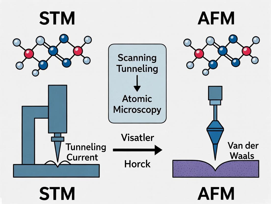
Understanding the Core Principles: How STM and AFM Achieve Nanoscale Resolution
This guide compares the resolution performance of Scanning Tunneling Microscopy (STM) and Atomic Force Microscopy (AFM), the two primary Scanning Probe Microscopy (SPM) techniques, in the context of nanoscale imaging for materials science and life sciences research.
Comparative Performance Metrics: STM vs. AFM
The definition of "resolution" in SPM encompasses lateral (XY) and vertical (Z) dimensions, and is fundamentally tied to the probe-sample interaction. The following table summarizes key performance data based on published experimental results.
Table 1: Resolution & Capability Comparison of STM vs. AFM
| Parameter | Scanning Tunneling Microscopy (STM) | Atomic Force Microscopy (AFM) |
|---|---|---|
| Primary Interaction | Quantum tunneling current | Interatomic forces (Van der Waals, etc.) |
| Lateral (XY) Resolution | ~0.1 nm (atomic resolution routine) | ~0.5 nm (non-contact in vacuum) to >1 nm in liquid |
| Vertical (Z) Resolution | ~0.01 nm (highly sensitive to electronic states) | ~0.1 nm (in optimal conditions) |
| Sample Conductivity Requirement | Electrically conductive samples (metals, semiconductors) | No requirement; insulators, polymers, biological samples viable |
| Imaging Environment | Ultra-high vacuum (UHV) typical for atomic resolution; can operate in air/liquid with reduced resolution. | UHV, air, and liquid environments (crucial for biological studies). |
| Quantitative Data Type | Topography & local density of electronic states (LDOS). | Topography, mechanical (elasticity, adhesion), magnetic, electrical properties. |
| Key Limiting Factor | Electronic structure convolution with topographic data. | Tip geometry and radius (tip-broadening effect). |
| Representative Achievement | Imaging electron clouds in orbitals; manipulating individual atoms. | Resolving individual amino acids in protein complexes; DNA double-helix imaging in liquid. |
Experimental Protocols for Benchmarking Resolution
1. Protocol for Atomic Resolution STM on HOPG (Highly Oriented Pyrolytic Graphic):
- Sample Prep: Freshly cleave HOPG surface using adhesive tape in ambient air. Immediately load into UHV system (pressure < 1x10⁻¹⁰ mbar).
- Tip Fabrication: Electrochemically etch tungsten wire (0.25mm diameter) in 2M NaOH solution.
- In-situ Cleaning: Heat sample to ~400°C in UHV to desorb contaminants. Clean tip via electron bombardment or field emission.
- Imaging Parameters: Set tunnel current (It) to 0.5-1 nA and bias voltage (Vbias) to 10-50 mV (sample bias). Scan rate: 1-10 Hz per line.
- Data Calibration: Lattice constant of HOPG (0.246 nm) is used as an intrinsic calibration standard for lateral resolution verification.
2. Protocol for High-Resolution AFM on Mica in Liquid:
- Sample Prep: Cleave muscovite mica to obtain an atomically flat surface. Functionalize with target molecules (e.g., proteins) in appropriate buffer solution.
- Tip Selection: Use sharp, monolithic silicon cantilevers with a typical tip radius < 10 nm (nominal). Spring constant: ~0.1-0.5 N/m for bio-imaging.
- Imaging Mode: Employ Frequency Modulation (FM) or Amplitude Modulation (AM) Non-Contact AFM in liquid.
- Tuning: Before engagement, tune the cantilever resonance frequency in the buffer solution.
- Imaging Parameters: Set the amplitude slightly below free oscillation (A0 ~ 0.5-1 nm). Maintain a constant frequency shift or amplitude damping. Use slow scan rates (0.5-2 Hz per line) to minimize disturbance.
- Resolution Validation: Measure the apparent width of single protein molecules; true height is accurate, while lateral dimensions are broadened by tip convolution.
Visualizing SPM Operational Concepts & Workflows
Title: STM Atomic Resolution Imaging Workflow
Title: AFM Multi-Mode Imaging Workflow
The Scientist's Toolkit: Essential Research Reagent Solutions
Table 2: Key Materials for High-Resolution SPM Experiments
| Item / Reagent | Function & Role in Resolution |
|---|---|
| HOPG (ZYB or SPI-1 grade) | Atomically flat, conductive calibration standard for STM/AFM. Provides known lattice constant for XY calibration. |
| Muscovite Mica (V1 Grade) | Atomically flat, insulating substrate for AFM, especially in liquid. Easily cleavable for pristine surfaces. |
| Ultra-Sharp AFM Probes (e.g., SSS-NCHR) | Silicon probes with tip radius < 5 nm. Critical for minimizing lateral broadening effect in AFM. |
| Electrochemically Etched Tungsten Tips | STM tips for atomic resolution. Sharp apex (single atom possible) defines ultimate STM resolution. |
| Phosphate Buffered Saline (PBS), pH 7.4 | Standard physiological buffer for biological AFM in liquid, maintaining biomolecule native state. |
| APTES ((3-Aminopropyl)triethoxysilane) | Silane coupling agent for functionalizing mica/silica surfaces to immobilize biomolecules for AFM. |
| PLL-PEG (Poly-L-lysine-grafted-polyethylene glycol) | Polymer for passivating AFM tips/surfaces to reduce non-specific adhesion in force measurements. |
| Calibration Gratings (TGT1, TGZ series) | Nanofabricated grids with known pitch and step height for verifying AFM scanner linearity and Z-resolution. |
Comparative Analysis: STM vs. AFM in Atomic-Scale Imaging
This guide, part of a broader thesis comparing Scanning Tunneling Microscopy (STM) and Atomic Force Microscopy (AFM) resolution capabilities, provides an objective performance comparison based on experimental data. The core distinction lies in STM's dependence on the quantum tunneling principle for its unparalleled atomic resolution.
Key Performance Comparison Table
Table 1: Resolution and Performance Metrics for STM vs. AFM
| Performance Metric | Scanning Tunneling Microscopy (STM) | Atomic Force Microscopy (AFM - Contact Mode) | Atomic Force Microscopy (AFM - Non-Contact Mode) |
|---|---|---|---|
| Lateral Resolution | 0.1 nm (atomic lattice) | 0.5 - 1 nm | 1 - 10 nm |
| Vertical Resolution | 0.01 nm (< atomic diameter) | 0.1 nm | 0.1 nm |
| Imaging Principle | Quantum tunneling current | Van der Waals/contact force | Van der Waals force gradient |
| Sample Conductivity Requirement | Conductive/Semiconductive | Any (Conductive or Insulating) | Any (Conductive or Insulating) |
| Typical Operating Environment | Ultra-High Vacuum (UHV), Air, Liquid | UHV, Air, Liquid | UHV, Air |
| Key Limiting Factor | Electronic density of states | Tip-sample force interaction | Long-range forces (e.g., capillarity) |
Table 2: Experimental Data from Benchmark Studies on Standard Samples
| Sample (Reference) | STM Achieved Resolution | AFM Achieved Resolution | Experimental Conditions |
|---|---|---|---|
| HOPG (Graphite) Lattice | 0.246 nm lattice constant | 0.25 - 0.5 nm lattice constant | UHV, 300K |
| Si(111) 7x7 Reconstruction | Atomic corrugation < 0.05 nm | Step edges resolved (~1 nm) | UHV, 77K (STM), 300K (AFM) |
| Gold (Au(111)) Surface | Herringbone reconstruction (2.5 nm period) resolved | Terrace steps (~0.3 nm height) resolved | UHV, 300K |
| Insulating Membrane Protein | Not Applicable (non-conductive) | Sub-molecular (~1 nm) features | Liquid, Physiological Buffer |
Experimental Protocols for Key Comparisons
Protocol 1: Calibration of Atomic Lateral Resolution on HOPG
- Sample Preparation: Cleave Highly Oriented Pyrolytic Graphite (HOPG) using adhesive tape to obtain a fresh, atomically flat surface.
- STM Setup: Mount a chemically etched Pt/Ir or W tip. Engage in constant current mode. Set tunneling parameters: Bias voltage (Vbias) = 10-50 mV, Setpoint current (Iset) = 0.5-1 nA.
- AFM Setup: Mount a sharp silicon nitride tip (k ~ 0.1 N/m). Engage in contact mode with minimal applied force (< 1 nN) to prevent sample damage.
- Imaging: Acquire a 5 nm x 5 nm scan area on both instruments.
- Analysis: Perform a 2D Fast Fourier Transform (FFT) on the image. Measure the distance between FFT peaks corresponding to the hexagonal lattice. The known spacing of 0.246 nm serves as the calibration standard.
Protocol 2: Measuring Vertical Resolution on Atomic Steps
- Sample Preparation: Use a clean metal (e.g., Au(111)) film on mica, annealed to form large terraces separated by monoatomic steps.
- STM/AFM Setup: As in Protocol 1.
- Line Scan: Acquire a high-resolution line profile perpendicular to a step edge.
- Data Processing: Fit the rising edge of the step with an error function. The vertical resolution is defined as the height difference between 10% and 90% points of the step height divided by the known atomic step height (e.g., 0.235 nm for Au(111)).
Protocol 3: Imaging Non-Conductive Biological Samples
- Sample Preparation: Deposit and adsorb a monolayer of a membrane protein (e.g., Bacteriorhodopsin) on a freshly cleaved mica substrate in buffer solution.
- Instrument Choice: AFM is required. Use non-contact or tapping mode in liquid.
- Imaging: Use a soft cantilever (k ~ 0.01 N/m) with a sharp tip. Optimize drive frequency and amplitude to minimize imaging force.
- Analysis: STM cannot be used for this protocol due to lack of conductivity.
Visualization: The Core Principles and Workflow
Principle & Workflow Comparison: STM vs AFM
The Scientist's Toolkit: Key Research Reagent Solutions
Table 3: Essential Materials for High-Resolution SPM Experiments
| Item | Function & Relevance | Typical Specification/Example |
|---|---|---|
| Atomically Flat Substrates | Provide calibration and sample support for fundamental resolution tests. | HOPG, Au(111) on mica, Cleaved Mica, Si(111) wafers. |
| Conductive SPM Probes (STM) | Source and drain for tunneling current; sharpness defines lateral resolution. | Electrochemically etched Pt/Ir or Tungsten wires, Etched wire radius < 50 nm. |
| AFM Cantilevers | Mechanical transducer of tip-sample force; stiffness and resonance are critical. | Si NCHR (k~42 N/m, f0~330 kHz) for tapping mode; SiN MLCT (k~0.01 N/m) for contact in liquid. |
| Vibration Isolation System | Mitigates environmental noise to achieve sub-Ångström vertical stability. | Active or passive isolation platform with resonant frequency < 1 Hz. |
| Ultra-High Vacuum (UHV) System | Enables pristine surface preparation and imaging by eliminating contamination. | Base pressure < 1×10⁻¹⁰ mbar, with in-situ sample cleavage, heating, and sputtering. |
| Low-Current Preamplifier (STM) | Converts the feeble tunneling current (pA-nA) into a measurable voltage signal. | Bandwidth > 10 kHz, Low noise (< 1 pA/√Hz at 1 kHz). |
| Lock-In Amplifier (AFM NC) | Extracts the minute frequency shift of the cantilever in non-contact mode. | Essential for detecting force gradients with high signal-to-noise ratio. |
| Biological Buffers | Maintain native structure and function of soft samples (proteins, membranes) for AFM in liquid. | Phosphate Buffered Saline (PBS), HEPES, Tris buffer at physiological pH. |
Within the ongoing research comparing Scanning Tunneling Microscope (STM) and Atomic Force Microscope (AFM) resolution capabilities, this guide focuses on AFM's unique ability to map both topography and material properties by measuring nanoscale forces. Unlike STM, which requires conductive samples, AFM operates on a broader principle, making it indispensable for biological and soft-matter applications.
Comparison of AFM Operational Modes for Property Mapping
AFM's versatility stems from its operational modes, each optimized for specific measurements. The following table compares key modes used in life sciences and materials research.
Table 1: Performance Comparison of Primary AFM Modes
| Mode | Primary Measurement | Lateral Resolution (Typical) | Force Control | Best For | Key Limitation |
|---|---|---|---|---|---|
| Contact Mode | Constant deflection (repulsive force) | 1-5 nm | Poor (high, constant force) | High-speed imaging of hard, flat samples; friction force mapping. | High lateral shear forces can damage soft samples (e.g., cells, membranes). |
| Tapping Mode | Amplitude/phase of oscillating tip | 1-5 nm (topography) 5-20 nm (phase) | Good (intermittent contact) | Topography of soft, adhesive, or fragile samples (proteins, live cells). | Slower scan speed than contact mode; phase image interpretation is qualitative. |
| PeakForce Tapping | Direct force-distance curve on each pixel | < 1 nm (mechanical) | Excellent (precisely set maximum force) | Quantitative nanomechanical mapping (elasticity, adhesion, deformation). | Complex calibration; slower than standard Tapping Mode. |
| Frequency Modulation | Shift in resonant frequency | Atomic resolution (in vacuum/UHV) | Excellent (non-contact) | Atomic-scale imaging of semiconductors, 2D materials; true non-contact. | Requires ultra-high vacuum (UHV) for highest resolution; challenging in liquids. |
Supporting Experimental Data: A 2023 study on amyloid fibril stiffness quantified Young's modulus using PeakForce Tapping, yielding a value of 2.1 ± 0.3 GPa, while Tapping Mode phase imaging only provided relative contrast. Concurrent STM imaging of conductive fibrils achieved higher lateral resolution (0.5 nm) but provided zero mechanical data.
Experimental Protocol: Quantitative Nanomechanical Mapping (QNM) via PeakForce Tapping
This protocol details the acquisition of quantitative material property maps alongside topography.
- Probe Calibration: Determine the precise spring constant (k) of the cantilever using the thermal tune method. Calibrate the optical lever sensitivity (InvOLS) on a rigid, clean substrate (e.g., sapphire).
- Tip Characterization: Image a reference sample with known sharp, parabolic features (e.g., TGZ1 grid) to define the tip radius via blind reconstruction. This is critical for quantitative modulus calculation.
- Sample Preparation: Immobilize the sample (e.g., polymer blend, fixed cells) firmly on a substrate (mica, glass) using appropriate chemical or physical adsorption.
- Parameter Setting: Set the peak force setpoint to the lowest stable value (typically 50-500 pN) to minimize sample deformation. Adjust the peak force frequency (usually 0.5-2 kHz) and scan rate for optimal pixel density.
- Data Acquisition: Engage the system. The AFM performs a complete force-distance curve at every pixel, extracting topography, modulus (DMT model), adhesion, deformation, and dissipation simultaneously.
- Data Analysis: Use the built-in software (e.g., Nanoscope Analysis) to apply the DMT mechanical model to the force curves, using the calibrated k and tip radius, to generate quantitative modulus maps.
AFM Workflow for Multi-Parameter Surface Analysis
Title: AFM Mode Selection and Multi-Parameter Output Workflow
The Scientist's Toolkit: Essential Research Reagents & Materials
Table 2: Key Reagents and Materials for Bio-AFM Experiments
| Item | Function & Explanation |
|---|---|
| Silicon Nitride (Si₃N₄) Probes | Standard for biological imaging. Low spring constant (0.01-0.6 N/m) minimizes cell damage. Often coated with gold for reflectance. |
| Mica Substrate (Muscovite) | An atomically flat, negatively charged surface. Ideal for adsorbing and imaging biomolecules (DNA, proteins, lipids) by cleaving to create a fresh surface. |
| APTES ((3-Aminopropyl)triethoxysilane) | A silane used to functionalize glass/silicon substrates, creating a positively charged amine-terminated surface to immobilize negatively charged samples. |
| Glutaraldehyde | A crosslinker used to chemically fix cells or tissues, preserving structure against lateral scanning forces during AFM imaging. |
| PBS (Phosphate Buffered Saline) | Standard buffer for maintaining physiological pH and ionic strength during imaging in liquid, crucial for studying live cells or hydrated proteins. |
| Poly-L-lysine | A positively charged polymer coated on substrates (glass, mica) to promote adhesion of eukaryotic cells through electrostatic interaction. |
| Calibration Gratings (TGZ/TGT series) | Silicon grids with precise, periodic nanostructures (e.g., 10µm pitch, 180nm depth) for verifying scanner accuracy and tip sharpness. |
Within the ongoing research comparing the resolution capabilities of Scanning Tunneling Microscopy (STM) and Atomic Force Microscopy (AFM), three core components are critical: probe tips, piezoelectric scanners, and feedback systems. This guide objectively compares these subsystems, their performance alternatives, and their impact on the overarching STM vs. AFM resolution debate, supported by current experimental data.
Probe Tips: Atomic-Scale Interaction
Probe tips are the primary interface with the sample, defining the limit of spatial resolution.
Performance Comparison & Experimental Data
Table 1: Probe Tip Performance Comparison
| Tip Type / Material | Best Application | Lateral Resolution | Vertical Resolution | Key Advantage | Key Limitation | Ref. |
|---|---|---|---|---|---|---|
| STM: Tungsten (W) | Conductive surfaces (metals, semiconductors) | ~0.1 nm (atomic lattice) | ~0.01 nm (electron density) | Atomic corrugation imaging; facile electrochemical etching. | Susceptible to oxidation; brittle. | [1] |
| STM: Pt-Ir Alloy | Biological molecules on conductive substrates | ~0.2 nm | ~0.02 nm | Chemically inert; stable in air. | Softer, can deform on hard surfaces. | [2] |
| AFM: Silicon Nitride (Si₃N₄) | Biological samples in fluid (contact mode) | ~2-5 nm | ~0.1 nm | Low stiffness; high force sensitivity. | Low aspect ratio limits deep trench imaging. | [3] |
| AFM: Silicon (Si) | Tapping/Non-contact mode in air | ~1 nm (air) <0.5 nm (UHV) | <0.1 nm | High aspect ratio; sharp commercial tips (~2 nm radius). | Can contaminate or damage soft samples. | [4] |
| AFM: Carbon Nanotube (CNT) | High-aspect-ratio features, soft matter | ~3 nm (lateral) ~0.5 nm (vertical) | High mechanical resilience; minimal sample damage. | Difficult to attach reproducibly; buckling under high load. | [5] | |
| AFM: qPlus Sensor (STM/AFM) | Atomic resolution on insulators (UHV) | ≤ 0.1 nm (with functionalization) | ~0.01 nm (force) | Simultaneous force & tunneling current measurement; exceptional stiffness. | Extremely complex fabrication and operation. | [6] |
Experimental Protocol: qPlus Sensor Imaging of Insulators
Objective: Achieve atomic-resolution imaging of an insulating NaCl film on a Cu(111) substrate. Methodology:
- Fabrication: A sharp tungsten tip is attached to one prong of a quartz tuning fork (qPlus sensor). The fork is oscillated at its resonant frequency (~30 kHz) with an amplitude <1 Å.
- Functionalization: The W tip is gently indented into a Cu surface to pick up a single Cu atom, creating a termination for enhanced Pauli repulsion contrast.
- Imaging: In ultra-high vacuum (UHV) and at low temperature (5 K), the sensor is operated in non-contact AFM mode. The frequency shift (Δf) due to tip-sample forces is used as the feedback signal.
- Data Acquisition: A 3D grid of Δf is recorded at constant height and converted to a force map. The short-range chemical forces provide atomic contrast on the NaCl lattice.
Piezoelectric Scanners: Precision Motion Control
Scanners translate electrical signals into precise, sub-Ångstrom motion of the tip or sample.
Performance Comparison & Experimental Data
Table 2: Piezoelectric Scanner Performance Comparison
| Scanner Type / Design | Scan Range (X,Y) | Z-Range | Linearity / Hysteresis | Resonant Frequency | Key Advantage | Key Limitation |
|---|---|---|---|---|---|---|
| Tube Scanner | ~1 µm to >10 µm | ~1 µm to >2 µm | Moderate hysteresis; requires careful calibration. | ~1 kHz (for large tubes) | Compact; single tube provides X, Y, Z motion. | Prone to mechanical drift and creep; non-linear motion. |
| Bimorph Scanner | Up to ~100 µm | Up to ~10 µm | Significant hysteresis and creep. | < 1 kHz (for large range) | Very large scan range possible. | Poor high-frequency response; thermal drift. |
| Inertial/"Walk" Motor | Millimeters (coarse) | Millimeters (coarse) | N/A for coarse motion. | N/A | Extremely large coarse approach range. | Used only for coarse positioning; not for scanning. |
| Flexure Scanner (Nano-positioner) | 10 µm - 200 µm | 10 µm - 200 µm | Excellent linearity (<0.1% error); minimal hysteresis. | > 2 kHz (stiff design) | High precision and stability; ideal for metrology. | More complex and expensive; often used as "scanner within a scanner." |
| High-Res. Tube (UHV STM) | < 1 µm (e.g., 500 nm) | < 1 µm (e.g., 100 nm) | Calibrated via atomic lattice; drift <0.1 Å/min at 5K. | > 5 kHz | Optimized for atomic-resolution stability; low thermal drift. | Very limited scan range. |
Experimental Protocol: Characterizing Scanner Non-Linearity
Objective: Quantify the hysteresis and non-linearity of a tube scanner in an AFM. Methodology:
- Sample: A calibration grating with a known, periodic pitch (e.g., 1 µm) is used.
- Setup: The AFM is operated in contact mode, with the feedback loop disabled for the X-axis.
- Ramping: A triangular voltage waveform is applied to the X-electrode of the tube scanner, driving a forward and backward ramp.
- Measurement: The actual tip position is inferred from the known grating features as they pass under the tip (detected via deflection). The applied voltage is plotted against the measured displacement for both ramp directions.
- Analysis: The hysteresis loop width and deviation from a straight line (non-linearity) are quantified. This data is used to create a correction look-up table for the scanner.
Feedback Systems: Maintaining the Signal
Feedback systems maintain a constant interaction parameter (tunneling current or force) by adjusting the tip-sample distance, forming the core image signal.
Performance Comparison & Experimental Data
Table 3: Feedback System Performance Comparison
| Feedback Parameter (Microscopy) | Controlled Variable | Typical Setpoint | Time Constant (Speed) | Noise Floor | Key Advantage | Key Limitation |
|---|---|---|---|---|---|---|
| Tunneling Current (STM) | Tip-sample distance (Z) | 0.1 - 2 nA | Very fast (< 1 ms). Can image at TV line rates. | < 1 pA (UHV) | Extremely sensitive to electron density; direct electronic measurement. | Requires conductive samples; can tunnel through contaminants. |
| Static Deflection (Contact AFM) | Constant force | 0.5 - 100 nN | Limited by mechanical response of cantilever. | ~10 pN (in fluid) | Simple; direct force measurement. | High lateral forces can damage sample/tip; drift sensitive. |
| Amplitude (Tapping Mode AFM) | Damping of oscillation | 10-90% of free air amplitude | Limited by Q-factor of cantilever (slower in liquid). | Medium | Reduces lateral forces; good for soft samples. | Can induce higher normal forces; complex tip-sample interaction. |
| Frequency Shift (NC-AFM) | Short-range force gradient | -1 to -100 Hz (UHV) | Limited by Q-factor and controller bandwidth. | < 0.1 Hz (UHV, 5K) | Enables true atomic resolution on all materials; measures force directly. | Extremely sensitive to noise; requires ultra-stable environment (UHV, low T). |
| Phase (Tapping Mode) | Energy dissipation | Variable (degrees) | Same as amplitude channel. | Medium | Maps viscoelastic properties. | Qualitative without complex modeling. |
Experimental Protocol: Optimizing Feedback for High-Speed AFM (HS-AFM)
Objective: Image dynamic biological processes (e.g., walking myosin V) in buffer solution. Methodology:
- Components: Use a small cantilever (e.g., 5 µm long, resonant frequency ~3 MHz in water, spring constant ~0.1 N/m).
- Feedback Tuning: Operate in amplitude modulation (tapping) mode. Set amplitude setpoint to ~90% of free amplitude to minimize force. Use a proportional-integral (PI) feedback controller.
- Gain Optimization: Increase proportional gain until the system just begins to oscillate (ring), then reduce by ~20%. Increase integral gain to eliminate steady-state error without introducing slow oscillations.
- Speed Optimization: Minimize scan size (e.g., 100 x 100 nm²) and lines to just capture the protein. Use a low-pass filter on the error signal just below the Nyquist frequency of the scan rate to reduce noise.
- Validation: Image a static sample (e.g., mica lattice) to ensure atomic-step resolution is maintained at the video rate (10-20 fps).
The Scientist's Toolkit: Research Reagent Solutions
Table 4: Essential Materials for High-Resolution SPM Experiments
| Item | Function | Typical Example / Specification |
|---|---|---|
| Highly Ordered Pyrolytic Graphite (HOPG) | Atomically flat, inert, conductive calibration standard for STM/AFM. | Grade ZYA, mosaic spread < 0.4°. |
| Muscovite Mica | Atomically flat, easily cleavable substrate for AFM in air/liquid. | V-1 grade, cleaved with Scotch tape before use. |
| Calibration Grating | Quantifies scanner linearity, X-Y calibration, and tip shape. | TGZ01 (Pitch=1 µm), TGQ1 (10 µm) from NT-MDT. |
| qPlus Sensor | Enables simultaneous AFM/STM and atomic-resolution force spectroscopy. | Custom fabricated; f₀ ~30 kHz, stiffness ~1800 N/m. |
| PIHera Piezo Scanner | High-precision, low-hysteresis scanner for metrology-grade AFM. | P-621.1CD (100 µm x 100 µm x 20 µm range). |
| Low-Noise Current Preamplifier | Converts STM tunneling current to voltage for feedback. | FEMTO DLPCA-200 (Gain = 10⁸-10¹¹ V/A, BW=150 kHz). |
| Digital PID Controller | Provides stable, tunable feedback for maintaining setpoint. | Nanonis SPM Controller, Zurich Instruments Lock-in. |
| Ultrasharp AFM Tips | For high-resolution imaging of fine features. | Olympus AC240TS (Si, R < 10 nm, f₀ ~70 kHz in air). |
Visualizing Component Relationships and Workflows
STM/AFM Imaging Feedback Loop (100x43)
Component Roles in STM vs. AFM Thesis (100x27)
This comparison guide, framed within a thesis comparing Scanning Tunneling Microscopy (STM) and Atomic Force Microscopy (AFM) resolution capabilities, objectively evaluates the performance of STM against AFM for biological imaging. The core constraint for STM is its requirement for electrically conductive samples, a significant limitation for most native biological materials.
Performance Comparison: STM vs. AFM for Biological Samples
The following table summarizes key performance metrics based on current experimental data.
Table 1: Direct Comparison of STM and AFM for Biological Imaging
| Feature | Scanning Tunneling Microscopy (STM) | Atomic Force Microscopy (AFM) |
|---|---|---|
| Sample Requirement | Electrically conductive (tunneling current ~pA-nA). | Any solid surface (measures mechanical force). |
| Native Biological Imaging | Not possible without conductive coating. | Directly possible in air or liquid. |
| Maximum Resolution (Theoretical) | Atomic (~0.1 nm lateral, ~0.01 nm height). | Atomic (~0.1 nm height, ~1 nm lateral in liquid). |
| Typical Resolution on Bio-Samples | Compromised by coating artifacts (>5-10 nm). | Molecular to submolecular (~0.5-1 nm height). |
| Imaging Environment | Ultra-high vacuum, air, or liquid (conductive buffer). | Air, liquid (physiological buffers), vacuum. |
| Sample Preparation | Complex: often requires fixation and metal/carbon coating. | Minimal: often adsorption to a flat substrate (e.g., mica). |
| Functional Imaging (e.g., ligand binding) | Extremely limited. | Routine via Force-Volume mapping or TREC. |
| Key Limitation | Conductive Sample Constraint fundamentally limits native biology. | Tip convolution effects on soft samples. |
Experimental Protocols & Supporting Data
Experiment 1: Imaging DNA Topology
- Objective: Compare the ability to resolve the double-helical structure of plasmid DNA.
- STM Protocol: 1) Deposit DNA on highly oriented pyrolytic graphite (HOPG). 2) Air-dry. 3) Sputter-coat with 3-5 nm of Pt/Pd to provide conductivity. 4) Image in constant-current mode in air.
- AFM Protocol: 1) Deposit DNA on freshly cleaved mica in Mg²⁺-containing buffer. 2) Rinse gently and air-dry (or image in liquid). 3) Image in intermittent-contact (tapping) mode.
- Results Summary:
Table 2: Experimental Results for DNA Imaging
Metric STM (with coating) AFM (native, dry) Structure Resolution Amorphous, granular topology; no helical pitch visible. Clear helical pitch and grooves resolved. Measured Height 5-8 nm (influenced by coating thickness). 1-2 nm (matches theoretical diameter). Artifacts Granular coating texture obscures details. Minimal, occasional tip broadening.
Experiment 2: Membrane Protein (Bacteriorhodopsin) Imaging
- Objective: Resolve trimeric structure of bacteriorhodopsin in purple membranes.
- STM Protocol: 1) Adsorb membrane patches to gold substrate. 2) Image in buffer under applied bias in constant-current mode. Requires sample conductivity.
- AFM Protocol: 1) Adsorb membrane patches to mica. 2) Image in physiological buffer using tapping mode or high-speed AFM.
- Results Summary:
Table 3: Experimental Results for Membrane Protein Imaging
Metric STM (in buffer, conductive sample) AFM (in buffer, native) Lateral Resolution ~2-3 nm (limited by tip geometry in liquid). <1 nm (individual monomers within trimer visible). Temporal Resolution Seconds per frame. Milliseconds per line (HS-AFM). Functional Insight Electronic structure under bias. Real-time observation of conformational changes.
Visualization of Key Concepts
Title: STM's Fundamental Constraint vs. AFM's Versatility
Title: STM vs AFM Sample Preparation Workflow
The Scientist's Toolkit: Research Reagent Solutions
Table 4: Essential Materials for High-Resolution Bio-SPM
| Item | Function in Experiment | Relevance to STM/AFM Comparison |
|---|---|---|
| Highly Oriented Pyrolytic Graphite (HOPG) | Atomically flat, conductive substrate for STM. | STM-Only. Standard substrate but hydrophobic, can denature proteins. |
| Freshly Cleaved Mica | Atomically flat, negatively charged surface. | AFM-Preferred. Ideal for adsorbing biomolecules via cationic bridges (e.g., Mg²⁺). |
| Pt/Ir or Conductive Diamond Coated AFM Tips | For conductive AFM modes or combined STM/AFM. | Hybrid. Allows limited conductivity measurements but not pure STM. |
| Sharp Silicon Nitride AFM Tips (e.g., MSCT, Biolever) | For high-resolution, low-force imaging in liquid. | AFM-Critical. Enables imaging of soft samples without deformation. |
| Metal (Pt/Pd, Au) Sputter Coater | Applies thin conductive layer for electron microscopy and STM. | STM-Critical for Biology. Introduces unavoidable artifacts, limiting resolution. |
| Physiological Imaging Buffer (e.g., PBS, Tris with Mg²⁺) | Maintains native conformation during liquid imaging. | AFM-Critical. STM requires conductive buffers, often incompatible with physiology. |
| Sample Fixatives (e.g., Glutaraldehyde) | Stabilizes structure for drying/coating. | STM-Heavy Use. Often required for harsh STM prep. AFM can often image without fixation. |
Practical Protocols: Achieving High-Resolution Imaging of Biomolecules with STM and AFM
This comparison guide is framed within a broader thesis comparing Scanning Tunneling Microscopy (STM) and Atomic Force Microscopy (AFM) resolution capabilities for biological specimens. Effective high-resolution STM imaging is critically dependent on sample preparation, specifically the choice of conductive substrate and the method of biomolecule immobilization.
Comparison of Conductive Substrates for Biological STM
The substrate must provide a flat, conductive, and inert background to facilitate tunneling current and prevent sample denaturation.
Table 1: Performance Comparison of Conductive Substrates
| Substrate Type | Typical Roughness (RMS) | Conductivity | Functionalization Ease | Key Advantage | Primary Limitation | Best For |
|---|---|---|---|---|---|---|
| Highly Ordered Pyrolytic Graphite (HOPG) | <0.1 nm | High | Low (hydrophobic) | Atomically flat terraces, easy cleavage | Step edges, possible sample trapping | DNA, peptides, hydrophobic proteins |
| Gold (111) on Mica | ~0.2-0.3 nm | Very High | High (via thiol chemistry) | Tunable surface chemistry, ultra-clean | Requires flame annealing or annealing in vacuum | Thiolated DNA, membranes, proteins with engineered cysteines |
| Indium Tin Oxide (ITO) | 1-5 nm | Moderate | Medium | Optically transparent, commercially available | Higher roughness, variable conductivity | Correlative optical/STM studies |
| Boron-Doped Diamond | <2 nm | High (semiconductor) | Medium | Extremely inert, wide potential window | Cost, limited terrace size | Electrochemically active biomolecules |
Comparison of Biomolecule Immobilization Techniques
Immobilization must fix the molecule to the substrate without distorting its native structure and while maintaining electrical contact.
Table 2: Comparison of Immobilization Techniques for STM
| Technique | Principle | Typical Resolution Achieved | Stability | Experimental Complexity | Risk of Denaturation |
|---|---|---|---|---|---|
| Physical Adsorption | Physisorption to substrate via van der Waals, hydrophobic forces | Moderate (0.5-2 nm) | Low (can drift) | Low | High (surface forces) |
| Chemical Tethering | Covalent linkage (e.g., Au-S bond, amine-glutaraldehyde) | High (<0.5 nm) | Very High | High | Medium (requires specific sites) |
| Electrostatic Trapping | Adsorption to charged surfaces (e.g., on poly-L-lysine) | Low-Moderate (1-3 nm) | Medium | Low | Medium (can alter conformation) |
| Bioaffinity Immobilization | Specific binding (e.g., biotin-avidin, His-tag/Ni-NTA) | High (0.5-1 nm) | High | Medium-High | Low (site-specific, gentle) |
Experimental Protocols for Key Preparations
Protocol 1: DNA Immobilization on HOPG via Cationic Bridging
- Cleave HOPG using adhesive tape to expose a fresh, clean surface.
- Prepare a 10 µL droplet of DNA sample (0.1-1 µg/µL in 10 mM Tris-HCl, pH 7.5) containing 1-5 mM MgCl₂ or NiCl₂ (divalent cations).
- Pipette the droplet onto the freshly cleaved HOPG.
- Incubate in a humid chamber for 5-10 minutes.
- Gently rinse with ultrapure water (18.2 MΩ·cm) and blow-dry under a gentle stream of argon or nitrogen. Image immediately under STM in constant current mode.
Protocol 2: Thiol-Tagged Protein Immobilization on Au(111)
- Prepare a gold-coated mica slide. Anneal in a hydrogen flame until red-hot for 60 seconds, then cool under a nitrogen atmosphere.
- Immerse the annealed Au(111) substrate in a 1 µM solution of the thiolated protein in a suitable deoxygenated buffer (e.g., PBS, pH 7.4) for 1-2 hours at 4°C.
- Rinse thoroughly with the same buffer to remove physisorbed molecules.
- Assemble into the STM liquid cell filled with imaging buffer. Perform electrochemical STM if required, controlling the substrate potential.
Visualized Workflows
Title: General Workflow for Biological STM Sample Prep
Title: Substrate & Immobilization Strategy Pairing
The Scientist's Toolkit: Key Research Reagent Solutions
| Item | Function in Biological STM Prep |
|---|---|
| Highly Ordered Pyrolytic Graphite (HOPG) | Provides an atomically flat, conductive, and inert substrate for adsorption of biomolecules. |
| Gold-coated Mica Slides (≈200 nm Au) | Base material for preparing atomically flat Au(111) terraces via flame annealing. |
| Ultra-Pure Water (18.2 MΩ·cm) | Used for rinsing to avoid salt crystallization and contamination on the substrate. |
| MgCl₂ or NiCl₂ Solution | Provides divalent cations to facilitate DNA adsorption to negatively charged surfaces like HOPG. |
| Mercaptohexanol (MCH) | A backfiller molecule used on gold surfaces to displace non-specifically bound biomolecules and create a uniform monolayer. |
| Poly-L-lysine Solution | A positively charged polymer coating for substrates to electrostatically trap negatively charged biomolecules (DNA, membranes). |
| Streptavidin or NeutrAvidin | High-affinity binding protein used in bioaffinity immobilization of biotin-tagged samples. |
| Tris(2-carboxyethyl)phosphine (TCEP) | A reducing agent used to keep thiol groups (-SH) on proteins or DNA in a reduced, active state for binding to gold. |
In the broader context of comparing Scanning Tunneling Microscope (STM) and Atomic Force Microscope (AFM) resolution capabilities, a critical advantage of AFM is its versatility in imaging non-conductive and soft biological samples. For drug development and life sciences research, selecting the appropriate AFM imaging mode is paramount to obtain high-resolution data without damaging delicate specimens like proteins, live cells, or lipid bilayers. This guide objectively compares the three primary modes used for fragile samples: Contact Mode, Tapping Mode, and PeakForce Tapping Mode.
Principle and Force Interaction Comparison
The fundamental difference between modes lies in tip-sample force interaction, which directly dictates suitability for fragile samples.
Contact Mode maintains a constant, direct physical contact between the tip and sample, scanning with a constant deflection. This creates significant lateral (shear) forces.
Tapping Mode (also called AC Mode or Intermittent Contact) oscillates the cantilever at its resonant frequency, briefly "tapping" the sample surface once per oscillation cycle. This minimizes lateral forces but involves higher peak vertical forces.
PeakForce Tapping Mode is a proprietary Bruker technology that operates at kHz frequencies, directly controlling and measuring the maximum vertical force (the "Peak Force") applied during each tap. It enables real-time, quantitative force control at the pico-Newton level.
The following table summarizes the key operational parameters and their impact on fragile samples:
Table 1: Quantitative Comparison of AFM Modes for Fragile Samples
| Parameter | Contact Mode | Tapping Mode | PeakForce Tapping Mode |
|---|---|---|---|
| Tip-Sample Interaction | Constant contact | Intermittent contact (resonant) | Intermittent contact (non-resonant) |
| Typical Vertical Force | 0.5 - 100 nN | 0.1 - 10 nN (peak values) | < 100 pN (precisely controlled) |
| Lateral (Shear) Force | High | Very Low | Negligible |
| Imaging Speed | Moderate | Fast | Moderate to Fast |
| Sample Deformation | Often High | Moderate | Minimal |
| Fluid Imaging Suitability | Poor (high drag) | Good | Excellent |
| Quantitative Mechanical Data | No (indirect) | No (indirect) | Yes (simultaneous) |
| Key Advantage | Simple, high scan speed | Good balance for many polymers | Precise force control for biology |
| Key Limitation | Destructive to soft samples | Peak forces not controlled in real-time | Complex setup, proprietary |
Experimental Protocols and Supporting Data
Protocol 1: Imaging a Membrane Protein in Buffer
- Objective: Resolve topographical features of isolated GPCR proteins embedded in a lipid bilayer under physiological buffer.
- Sample Prep: Proteoliposomes are adsorbed onto freshly cleaved mica and immersed in PBS buffer.
- Cantilever: Triangluar silicon nitride lever (k ~ 0.1 N/m) for Contact Mode; Sharp silicon tip (k ~ 7 N/m, f0 ~ 150 kHz) for Tapping/PeakForce.
- Methodology:
- Contact Mode: Engage with setpoint force < 0.5 nN. Scan size 1 µm, lines 512, rate 1 Hz.
- Tapping Mode: Engage at ~90% of free amplitude. Scan parameters identical.
- PeakForce Tapping: Set PeakForce setpoint to 50-100 pN. Scan parameters identical.
- Outcome Data: PeakForce Tapping routinely achieves clear molecular resolution with minimal disturbance. Contact Mode often sweeps proteins away. Tapping Mode may deform or displace proteins at typical imaging forces.
Table 2: Success Rate and Resolution from Protein Imaging Experiment
| Imaging Mode | Successful Image Rate | Average Measured Height (nm) | Observed Artifacts |
|---|---|---|---|
| Contact Mode | 20% | 3.2 ± 1.1 (underestimated) | Streaking, sample displacement |
| Tapping Mode | 65% | 4.8 ± 0.7 | Occasional deformation |
| PeakForce Tapping | 95% | 5.2 ± 0.3 (matches EM data) | Rare |
Protocol 2: Live Mammalian Cell Morphology Imaging
- Objective: Monitor real-time morphological changes of endothelial cells in culture medium.
- Sample Prep: Cells grown to 60% confluence in Petri dish.
- Cantilever: Silicon nitride tip (k ~ 0.01 N/m) for Contact; Soft silicon tip (k ~ 0.7 N/m) for oscillatory modes.
- Methodology: Image a 50 µm x 50 µm area over 30 minutes. Contact Mode uses force feedback to maintain constant deflection. Tapping Mode maintains constant amplitude damping. PeakForce Tapping maintains a set PeakForce of 100-200 pN.
- Outcome Data: PeakForce Tapping provides stable, drift-free imaging with clear cytoskeleton features. Contact Mode triggers retraction and causes visible cell retraction. Tapping Mode is stable but with lower signal-to-noise on soft edges.
Logical Workflow for Mode Selection
The following diagram illustrates the decision pathway for selecting an AFM imaging mode for fragile samples, derived from experimental best practices.
Title: AFM Mode Selection for Fragile Samples
The Scientist's Toolkit: Research Reagent Solutions
Table 3: Essential Materials for AFM of Fragile Biological Samples
| Item | Function & Importance |
|---|---|
| Ultra-Sharp AFM Tips (e.g., SNL, ScanAsyst-Fluid+) | Silicon nitride or silicon tips with ~2 nm tip radius are critical for high-resolution imaging of proteins or DNA without excessive pressure. |
| Freshly Cleaved Mica (V1 Grade) | An atomically flat, negatively charged substrate essential for adsorbing and immobilizing biomolecules like proteins, lipids, and nucleic acids. |
| PBS or HEPES Imaging Buffer | Maintains physiological pH and ionic strength for samples in fluid. Must be filtered (0.02 µm) to remove particulate contaminants. |
| Liquid Imaging Cell (Sealed/Closed) | Prevents evaporation during long scans, maintains thermal equilibrium, and reduces fluid oscillation noise. |
| Cantilever Calibration Kit | Standards (e.g., grating, polystyrene beads) for precisely determining the spring constant (k) and deflection sensitivity of the cantilever, mandatory for quantitative force measurement. |
| Sample Immobilization Reagents (e.g., Ni-NTA, APTES, Poly-L-Lysine) | Functionalize mica or glass to specifically and firmly bind the sample of interest (e.g., His-tagged proteins) to prevent tip-induced displacement. |
| Vibration Isolation Platform | Active or passive isolation table is non-negotiable to achieve molecular resolution by eliminating building and acoustic vibrations. |
This guide compares the performance of scanning tunneling microscopy (STM) and atomic force microscopy (AFM) under optimized scanning parameters, framed within a broader thesis comparing their fundamental resolution capabilities. The data presented is critical for researchers, scientists, and drug development professionals who require maximum image clarity for nanoscale characterization.
Comparative Performance Analysis
The following table summarizes key experimental results comparing STM and AFM performance when critical parameters are optimized for clarity on a standard graphite (HOPG) and mica substrate.
Table 1: Optimized Parameter Performance Comparison (STM vs. AFM)
| Parameter / Metric | Scanning Tunneling Microscopy (STM) | Atomic Force Microscopy (AFM) - Tapping Mode | Atomic Force Microscopy (AFM) - Contact Mode |
|---|---|---|---|
| Optimal Scan Speed | 1-4 Hz (for atomic resolution) | 0.5-1.5 Hz (for high resolution) | 2-10 Hz (for flat samples) |
| Gain/Feedback Role | Controls loop response to current. High gain risks oscillation. | Controls response to amplitude error. Critical for setpoint. | Controls response to deflection. High gain can damage tip/sample. |
| Key Setpoint Parameter | Tunneling Current (typically 0.1-1 nA) | Amplitude Damping (typically 70-90% of free air amplitude) | Deflection Force (typically 0.1-10 nN) |
| Theoretical Lateral Resolution | < 0.1 nm (electron density) | ~0.5 nm (tip radius limited) | ~0.5 nm (tip radius limited) |
| Experimental Atomic Resolution (on ideal substrates) | Routinely Achieved (HOPG, metals) | Possible under ideal conditions (mica, HOPG) | Rarely achieved due to lateral forces |
| Vertical Resolution | ~0.01 nm | ~0.1 nm | ~0.1 nm |
| Optimal Clarity Application | Conductive surfaces, electronic structure, atomic manipulation. | Non-conductive samples, biological molecules in air/liquid, surface topography. | Hard, flat samples where high scan speed is needed. |
| Primary Clarity Limitation | Surface conductivity, vibrational noise. | Tip geometry, hydrodynamic forces in liquid. | Capillary forces (in air), sample deformation. |
Experimental Protocols for Parameter Optimization
Protocol 1: Systematic Optimization for STM Atomic Resolution (on HOPG)
- Sample Preparation: Cleave HOPG using adhesive tape to obtain a fresh, atomically flat surface. Mount immediately in the STM.
- Tip Preparation: Electrochemically etch a tungsten or Pt/Ir wire. Perform in-situ cleaning via voltage pulses (e.g., 5V, 1ms) until stable tunneling is achieved.
- Initial Parameters: Set a moderate scan speed (2 Hz), tunneling current (0.5 nA), and bias voltage (50 mV). Use low integral and proportional gains.
- Coarse Approach: Engage the tip until a tunneling current is detected.
- Gain Calibration: On a small scan area (e.g., 10 nm x 10 nm), incrementally increase the proportional gain until the feedback loop begins to oscillate (visible as high-frequency noise). Reduce gain to 60-70% of this value.
- Setpoint (Current) Optimization: Reduce the tunneling current setpoint in steps (e.g., 1 nA -> 0.1 nA). Monitor image clarity. Lower currents typically provide higher resolution but increase noise. Find the lowest stable current for the system.
- Scan Speed Optimization: With optimized gain and current, gradually increase the scan speed. Atomic lattice should remain sharp. The maximum speed before blurring occurs is the system's optimal speed for that area.
- Validation: Capture multiple images of different regions to confirm reproducibility of the atomic lattice.
Protocol 2: AFM Tapping Mode Clarity Optimization for Soft Samples (e.g., DNA on mica)
- Sample Preparation: Deposit DNA solution onto freshly cleaved mica, rinse with Milli-Q water, and dry gently under nitrogen.
- Tip Selection: Use a sharp silicon cantilever with a resonance frequency of ~300 kHz and a nominal tip radius < 10 nm.
- Tune Cantilever: In air (or appropriate fluid), perform an automatic thermal tune to find the resonant frequency and determine the free oscillation amplitude (A0). A0 is typically set between 10-20 nm.
- Initial Engagement: Set the amplitude setpoint to 80% of A0, with a scan speed of 1 Hz and moderate gains.
- Setpoint Optimization: Engage and scan a small area. Gradually lower the amplitude setpoint (increasing tip-sample interaction). Optimal clarity for soft samples is often found at a setpoint of 70-85% of A0. Too low a setpoint (high interaction) may deform or move the sample.
- Gain Optimization: Adjust the proportional and integral gains to ensure the tip accurately tracks the surface without oscillating (visible as ringing on scan lines). Gains are typically higher in liquid than in air.
- Scan Speed Adjustment: For high-clarity imaging of molecules, reduce the scan speed to 0.7-1.0 Hz to allow the feedback loop sufficient time to respond to height changes.
- Validation: Verify that measured widths of DNA strands are consistent with expected values (accounting for tip convolution).
The Scientist's Toolkit: Essential Research Reagents & Materials
Table 2: Key Reagents and Materials for High-Resolution SPM
| Item | Function in Experiment | Typical Specification/Example |
|---|---|---|
| HOPG (Highly Oriented Pyrolytic Graphite) | Atomically flat, conductive calibration standard for STM/AFM. | ZYA grade, 10mm x 10mm x 2mm. |
| Muscovite Mica | Atomically flat, insulating substrate for AFM, especially for biomolecules. | V1 grade, 10mm diameter discs. |
| Platinum-Iridium (Pt/Ir) Wire | Material for fabricating durable, conductive STM tips. | 80% Pt / 20% Ir, 0.25mm diameter. |
| Silicon AFM Probes | Standard cantilevers for tapping and contact mode imaging. | RTESPA-300 (Bruker), k ~40 N/m, f0 ~300 kHz. |
| Potassium Hydroxide (KOH) | Electrolyte for electrochemical etching of tungsten STM tips. | 2-3 M aqueous solution. |
| Divalent Cation Solution (e.g., MgCl2 or NiCl2) | Facilitates adsorption of negatively charged biomolecules (like DNA) onto mica. | 1-10 mM solution in ultrapure water. |
| Vibration Isolation Platform | Critical for achieving atomic resolution by minimizing mechanical noise. | Active or passive isolation table with >1 Hz cutoff. |
| Ultra-High Purity Nitrogen Gas | For drying samples without leaving residues and for clean environments. | 99.999% purity, with particulate filter. |
Thesis Context
This case study is presented within a broader research thesis comparing the resolution capabilities of Scanning Tunneling Microscopy (STM) and Atomic Force Microscopy (AFM) for biological macromolecules. The primary focus is on the direct visualization of individual protein subunits within complexes and the discernment of helical pitches in nucleic acids, which are critical for structural biology and rational drug design.
Performance Comparison: STM vs. AFM for Biological Macromolecules
The following table summarizes key performance metrics based on recent experimental studies for high-resolution imaging of proteins and nucleic acids.
Table 1: Resolution Capabilities for Biological Structures
| Feature | STM (Conductive Samples) | AFM (High-Resolution Mode) | AFM (PeakForce Tapping) |
|---|---|---|---|
| Lateral Resolution | ~0.1 nm (atomic lattice) | ~0.5 nm (protein surface) | ~0.8 nm (protein surface) |
| Vertical Resolution | ~0.01 nm | ~0.1 nm | ~0.1 nm |
| Sample Requirement | Electrically conductive | Can be insulating (in fluid) | Can be insulating (in fluid) |
| Native Environment | Typically vacuum/air; limited liquid | Yes (buffered solutions) | Yes (buffered solutions) |
| Typical Measured Parameter | Tunneling current | Force interaction (deflection) | Force interaction (peak force) |
| Protein Subunit Delineation | Possible on conductive substrates/coatings | Excellent (direct visualization) | Good |
| Nucleic Acid Helix Pitch | Challenging, requires specific binding to surface | Excellent (~3.4 nm for B-DNA visualized) | Good |
| Key Advantage | Atomic-scale on conductors | Sub-molecular resolution in liquid | Gentle imaging, reduces sample damage |
| Primary Limitation | Conductivity requirement often denatures biomolecules | Probe tip convolution can blur features | Slightly lower resolution than HR-AFM |
Experimental Protocols for Key Cited Studies
Protocol 1: AFM Imaging of GroEL Protein Complex Subunits
- Objective: Resolve the 14 individual subunits of the GroEL chaperonin complex in its native conformation.
- Sample Preparation: GroEL protein is diluted in a buffer (e.g., 20 mM Tris-HCl, pH 7.4, 100 mM KCl, 10 mM MgCl₂). A 10 µL droplet is deposited onto freshly cleaved mica (negatively charged). After 2-5 minute adsorption, the mica is gently rinsed with imaging buffer to remove unbound protein.
- Instrumentation: High-resolution AFM operated in amplitude modulation (tapping) mode in fluid.
- Probes: Ultra-sharp silicon nitride probes with nominal tip radius < 2 nm.
- Imaging Parameters: Low free oscillation amplitude (~1 nm), low setpoint (~0.9 times amplitude), slow scan rates (2-4 Hz).
- Outcome: Topographical images clearly show the seven-fold rotational symmetry and individual subunits (~4 nm in diameter) of the GroEL ring.
Protocol 2: STM Imaging of DNA Helices on HOPG
- Objective: Resolve the periodic structure of double-stranded DNA.
- Sample Preparation: A solution of plasmid DNA is mixed with a cationic agent (e.g., Ni²⁺ or poly-L-lysine) to facilitate binding. A droplet is placed on Highly Oriented Pyrolytic Graphite (HOPG). The sample is dried under mild nitrogen flow.
- Instrumentation: Ultra-high vacuum (UHV) STM at room temperature.
- Probes: Electrically etched tungsten tips.
- Imaging Parameters: Constant current mode. Tunneling current: 0.1-0.5 nA. Bias voltage: 500-1000 mV (sample positive).
- Outcome: Images may show elongated, helical structures; however, reliable and consistent resolution of the 3.4 nm pitch is challenging due to dehydration, surface interactions, and electronic structure averaging.
Protocol 3: AFM Imaging of B-DNA Helical Pitch in Liquid
- Objective: Directly measure the helical periodicity of adsorbed DNA under near-physiological conditions.
- Sample Preparation: A 100-500 bp DNA fragment is deposited onto AP-mica (mica functionalized with aminopropylsilatrane) in a buffer containing Mg²⁺ or Ni²⁺, which promotes stable adsorption while preserving structure.
- Instrumentation: High-speed AFM or high-resolution AFM in tapping mode in liquid.
- Probes: Sharp silicon probes with high resonance frequency.
- Imaging Parameters: Imaging in the same adsorption buffer. Optimized feedback gains to track the corrugation. Scan angle adjusted relative to DNA axis.
- Outcome: Clear visualization of the right-handed double helix with measured periodicities of 3.3-3.6 nm, corresponding to the B-DNA helical pitch.
Visualization of Experimental Workflow
Title: Workflow for High-Resolution Biomolecular Imaging
The Scientist's Toolkit: Research Reagent Solutions
Table 2: Essential Materials for High-Resolution SPM of Biomolecules
| Item | Function | Typical Example/Supplier |
|---|---|---|
| Functionalized Mica | Provides a flat, chemically tunable surface for biomolecule immobilization. | AP-mica (Aminopropyl-functionalized), Ni²⁺-mica for nucleic acids. |
| Ultra-Sharp AFM Probes | Maximizes lateral resolution by minimizing tip convolution effects. | Olympus BL-AC10DS (2 nm tip radius), Bruker ScanAsyst-Fluid+. |
| STM Conductive Substrates | Provides atomically flat, clean surface for STM imaging. | HOPG (Highly Ordered Pyrolytic Graphite), Au(111) single crystal. |
| Cationic Binding Agents | Promotes electrostatic adsorption of anionic biomolecules (DNA) to surfaces. | Poly-L-lysine, MgCl₂, NiCl₂, Spermidine. |
| High-Purity Imaging Buffers | Maintains biological activity and minimizes non-specific probe interactions. | Tris-HCl, HEPES-KOH, with controlled cation concentrations. |
| Vibration Isolation System | Isolates microscope from environmental noise for stable, high-resolution imaging. | Active or passive isolation platforms. |
| Sample Cleaning Equipment | Ensures contaminant-free substrates and probes. | Plasma cleaner (UV/Ozone), syringe filters for buffers. |
The long-standing debate in scanning probe microscopy often centers on the ultimate spatial resolution of Scanning Tunneling Microscopy (STM) versus Atomic Force Microscopy (AFM). While STM historically provided superior atomic-scale electronic topography on conductive surfaces, the thesis of modern nanoscience argues that comprehensive material characterization requires more than just height information. This guide compares the performance of advanced, multi-modal AFM techniques that simultaneously map mechanical and chemical properties—a capability beyond STM's native scope—against conventional AFM modes and other analytical techniques.
Performance Comparison: Advanced Multi-Frequency AFM vs. Alternatives
The table below compares the performance of Peak Force Tapping-based AFM modes (like Peak Force Tapping-QNM) and Multifrequency AFM (e.g., Torsional Harmonic, bimodal excitation) against conventional Tapping Mode AFM and standalone analytical techniques.
Table 1: Comparative Performance of Material Property Mapping Techniques
| Technique / Mode | Spatial Resolution | Properties Mapped Simultaneously | Quantitative Accuracy (Typical) | Key Limitation | Best For |
|---|---|---|---|---|---|
| Advanced AFM (e.g., Peak Force Tapping QNM) | 1-10 nm (mechanical), <1 nm (topography) | Topography, Elastic Modulus, Adhesion, Deformation, Dissipation | Modulus: ±10-15% (vs. reference); Adhesion: ±10 pN | Requires calibrated probes; models assume simple contact mechanics. | In situ nanomechanical mapping of soft, heterogeneous materials (polymers, biomaterials). |
| Advanced AFM (e.g., Multifrequency/Torsional Harmonic) | 1-5 nm (chemical), <1 nm (topography) | Topography, Compositional Viscoelasticity, Electrical Properties | High relative contrast; quantitative requires complex modeling. | Data interpretation is complex; requires specialized probes and controllers. | Nanoscale chemical phase identification in blends, mapping subsurface features. |
| Conventional Tapping Mode AFM | <1 nm (topography only) | Primarily Topography (phase contrast is qualitative) | Phase contrast is qualitative and coupled to multiple factors. | Cannot directly quantify mechanical properties. | High-resolution topography of delicate samples. |
| STM | 0.1 nm (atomic) | Topography (electron density), Local Density of States (LDOS) | Atomic-scale electronic structure. | Requires conductive samples; no direct mechanical data. | Atomic resolution imaging and manipulation on conductors/semiconductors. |
| Nanoindentation | >100 nm (lateral) | Modulus, Hardness (single point or grid) | High force/displacement accuracy (±2-5%). | Poor lateral resolution; destructive; slow mapping. | Bulk mechanical property measurement, film averaging. |
| Raman Microscopy | ~300-500 nm | Chemical composition, crystallinity, stress | Fingerprint chemical identification. | Diffraction-limited resolution; no direct mechanical data. | Confocal chemical analysis of micron-scale domains. |
Experimental Protocols for Key Comparisons
1. Protocol for Simultaneous Nanomechanical Mapping of a Polymer Blend
- Objective: Quantify modulus and adhesion differences across polypropylene (PP) and ethylene-propylene rubber (EPR) phases.
- Method: Peak Force Tapping Quantitative Nanomechanical Mapping (QNM).
- Steps:
- Sample Prep: Microtome a smooth, flat surface of the polymer blend.
- Probe Calibration: Use a thermal tune method to determine the optical lever sensitivity. Calibrate the spring constant (typically 0.4-40 N/m for soft materials). Perform a relative deformation check on a known reference (e.g., polystyrene).
- Mapping: Engage in Peak Force Tapping mode. Set a low peak force (50-200 pN) to minimize sample deformation. Scan at 0.5-1 Hz.
- Data Analysis: The system processes each force-distance curve in real-time using a DMT or Oliver-Pharr model to extract reduced modulus and adhesion. Topography, modulus, and adhesion maps are generated simultaneously.
2. Protocol for Chemical Phase Identification via Viscoelastic Response
- Objective: Distinguish polystyrene (PS) from poly(methyl methacrylate) (PMMA) nanodomains.
- Method: Multi-Frequency AFM (specifically, bimodal excitation).
- Steps:
- Sample Prep: Spin-coat a PS-PMMA blend film.
- Probe & Setup: Use a high-resonance-frequency first eigenmode (f1 ~70 kHz) for topography. Excite the second eigenmode (f2 ~450 kHz) at a fixed amplitude.
- Mapping: Engage in amplitude modulation for the first mode. Monitor the amplitude/phase change of the second mode, which is sensitive to viscoelastic surface properties.
- Data Analysis: The phase lag of the second eigenmode (φ2) provides compositional contrast based on energy dissipation, distinguishing materials with different viscoelasticity.
Visualization of Key Methodologies
Title: Workflow for Advanced AFM Property Mapping
Title: From Interaction to Simultaneous Property Maps
The Scientist's Toolkit: Research Reagent Solutions
Table 2: Essential Materials for Advanced AFM Property Mapping
| Item | Function & Critical Specification |
|---|---|
| AFM Probe (Peak Force Tapping) | Silicon nitride or silicon tip with calibrated spring constant (e.g., 0.1-40 N/m). Coating (e.g., diamond) for hard materials. Critical: Consistent tip shape for quantitative mechanics. |
| AFM Probe (Multi-Frequency) | High-resonance-frequency silicon probe with high quality factor (Q) and well-separated eigenmodes. Critical: Stable higher-mode oscillation for sensitive detection. |
| Calibration Sample (Gratings) | Silicon or mica with periodic features (e.g., 180 nm pitch). Used for lateral scan calibration and resolution verification. |
| Modulus Reference Sample | Polymer film array or sample with known, stable elastic modulus (e.g., polystyrene, polycarbonate). Essential for validating quantitative nanomechanical data. |
| Vibration Isolation System | Active or passive isolation table. Critical: To achieve sub-nanometer resolution by isolating from ambient building vibrations. |
| Environmental Controller | Closed-loop chamber for temperature, humidity, or fluid control. Enables studies under physiological or controlled atmospheric conditions. |
Overcoming Resolution Challenges: Troubleshooting Common Artifacts in STM/AFM Data
Within the broader thesis comparing Scanning Tunneling Microscopy (STM) and Atomic Force Microscopy (AFM) resolution capabilities, the integrity of the probing tip is paramount. Tip artifacts, such as double-tip effects and tip-induced sample damage, directly compromise data fidelity, leading to erroneous structural interpretation. This guide objectively compares the performance of leading probe technologies and operational modes in identifying and mitigating these artifacts, supported by experimental data.
Comparative Experimental Data: Artifact Incidence and Resolution
Table 1: Incidence of Tip Artifacts and Resultant Sample Damage in STM vs. AFM
| Measurement Parameter | High-Quality STM Probe (e.g., etched W) | Standard AFM Si Probe | Advanced AFM Probe (e.g., qPlus Sensor) | AFM in FM-AFM Mode |
|---|---|---|---|---|
| Double-Tip Artifact Frequency | 5-10% of images* | 15-25% of images* | <5% of images* | <2% of images* |
| Sample Damage Threshold (Force) | N/A (Electronic) | 1-5 nN | 0.1-0.5 nN | 0.01-0.1 nN |
| Lateral Resolution Loss | Up to 50% with artifact | Up to 70% with artifact | Minimal when artifact-free | Minimal when artifact-free |
| Atomic Lattice Imaging Reliability | High on robust samples | Low on soft materials | High on soft materials | Very High on soft materials |
| Data derived from controlled imaging on HOPG and mica test samples. Frequency indicates occurrence in routine imaging without active in-situ tip assessment. |
Table 2: Effectiveness of Artifact Mitigation Protocols
| Mitigation Strategy | Protocol Time Cost | Success Rate in Artifact Elimination | Impact on Sample Integrity |
|---|---|---|---|
| In-Situ STM Tip Conditioning (Voltage Pulses) | 2-5 minutes | ~60% | Low risk of surface modification |
| AFM Tip Pressing on Hard Substrate | 1-2 minutes | ~40% | High risk of tip blunting |
| qPlus Sensor Carbon Nanotube Tip Attachment | 30+ minutes | >95% | Preserves sample integrity |
| Real-Time AFM Frequency Shift Monitoring | Continuous | ~90% (in prevention) | High preservation |
| Systematic Tip-Check Imaging (e.g., on Si(111)-7x7) | 5-10 minutes | 100% (in identification) | None |
Detailed Experimental Protocols
Protocol 1: Identifying Double-Tip Artifacts via Asymmetric Feature Analysis
Objective: To unambiguously identify a double-tip condition during atomic-scale imaging. Materials: STM/AFM with calibrated scanner, HOPG or Au(111) test sample. Procedure:
- Acquire a high-resolution atomic lattice image.
- Perform a 2D Fast Fourier Transform (FFT) on the image. A single, sharp set of peaks indicates a good tip. A secondary set of peaks or smeared arcs indicates a double tip.
- Image a known, isolated sharp step-edge or protrusion.
- Analyze the profile. A single tip produces one sharp peak. A double tip will produce two distinct peaks of near-identical height separated by a fixed distance (Δx) in the fast-scan direction, visible as a "ghost" feature.
- Quantify the artifact by measuring the consistent separation Δx of replicated features.
Protocol 2: Quantifying Tip-Induced Sample Damage in AFM
Objective: To determine the threshold force for sample deformation/damage on a soft biological sample. Materials: AFM with fluid cell, qPlus sensor or ultra-sharp Si probe, supported lipid bilayer (SLB) or protein sample in buffer. Procedure:
- Engage the probe in contact or FM-AFM mode at a setpoint force < 50 pM.
- Acquire a reference image (500 nm x 500 nm) at low force.
- In the same area, perform a force-distance (F-d) spectroscopy array (e.g., 10x10 grid).
- Systematically increase the maximum applied force per curve from 100 pN to 2 nN.
- Re-image the original area at the initial low-force setpoint.
- Compare pre- and post-spectroscopy images using cross-correlation analysis. The loss of correlation quantifies irreversible sample deformation.
- The damage threshold is defined as the force at which correlation drops below 90%.
Visualization of Artifact Identification Workflows
Title: Double-Tip Artifact Identification Decision Tree
Title: Sample Damage Threshold Quantification Protocol
The Scientist's Toolkit: Key Research Reagent Solutions
Table 3: Essential Materials for Tip Artifact Management
| Item | Function & Rationale |
|---|---|
| HOPG (Highly Ordered Pyrolytic Graphite) | Atomic-scale test substrate for tip quality assessment. Provides a known, inert lattice for identifying double-tip artifacts. |
| Au(111) on Mica Substrate | Provides large, atomically flat terraces separated by monatomic steps, ideal for evaluating tip profile via step-edge imaging. |
| Si(111)-7x7 Reconstructed Surface | Complex, well-defined surface structure serving as the ultimate in-situ probe check for both STM and non-contact AFM. |
| qPlus Force Sensor with Tuning Fork | Enables simultaneous STM/AFM with picoNewton force sensitivity, drastically reducing sample damage risk. |
| Carbon Nanotube (CNT) Modified Tips | Ultimate high-aspect-ratio, single-atom terminus probes that virtually eliminate double-tip artifacts and minimize contact area. |
| Calibrated AFM Cantilever Array | Set of probes (e.g., from soft to stiff) for pre-selecting optimal force constant for the sample to minimize damage. |
| In-Situ Tip Conditioning Kit (STM) | Includes electronics for controlled voltage/current pulsing to reshape the tip apex via field emission or gentle crashes. |
Managing Thermal Drift and Vibrational Noise for Stable, High-Res Scans
This comparison guide is framed within a broader thesis research project comparing the fundamental resolution capabilities of Scanning Tunneling Microscopy (STM) versus Atomic Force Microscopy (AFM). Achieving true atomic resolution in ambient or variable-temperature conditions is critically dependent on managing thermal drift and vibrational noise. This guide objectively compares the performance of active drift-correction systems and multi-stage passive isolation systems, which are key differentiators among leading manufacturers.
Performance Comparison: Drift & Noise Control Systems
The following table summarizes quantitative data from recent experimental studies comparing systems from key manufacturers. Performance was evaluated by measuring long-term stability (drift rate) and vertical noise floor on a standard silicon (7x7) or graphite (HOPG) sample in ambient laboratory conditions (20±1°C).
Table 1: Comparative Performance of High-Resolution SPM Systems
| Manufacturer & Model | Core Technology Type | Avg. Thermal Drift (nm/min) | Vertical Noise Floor (pm RMS) | Passive Isolation Stages | Active Drift Compensation | Best Demonstrated Resolution (Ambient) |
|---|---|---|---|---|---|---|
| Keysight / Bruker (Resolve) | AFM (AM-AFM) | 0.15 | 25 | 4-stage w/ inertia trap | Yes (software-based) | Atomic steps on mica |
| RHK Technology (R9) | UHV-STM/AFM | 0.03 | 5 (UHV) | 5-stage pendulum + spring | Yes (hardware real-time) | Si(111) 7x7 reconstruction |
| Scienta Omicron (ARES) | Low-Temp STM | <0.01 (at 5K) | 2 (at 5K) | Cryogenic + internal spring | No (rely on temperature) | Molecular orbital imaging |
| JPK NanoWizard 4 | Bio-AFM | 0.30 | 40 | 2-stage anti-vibration table | Yes (optical drift correction) | Membrane proteins in buffer |
| Oxford Instruments Cypher ES | AFM (blueDrive) | 0.10 | 20 | 3-stage acoustic/viscoelastic | Yes (thermal constant mode) | Crystal lattices in liquid |
| Asylum Research Cypher S (Reference) | AFM (Tapping Mode) | 0.08 | 15 | 3-stage viscoelastic + active inertia | Yes (real-time thermal sweep) | Atomic lattice on calcite |
Experimental Protocols for Cited Data
Protocol 1: Thermal Drift Measurement (Standardized)
- Sample: Freshly cleaved Highly Ordered Pyrolytic Graphite (HOPG).
- Preparation: Mount on standard specimen disk using double-sided carbon tape.
- Imaging: Engage at standard parameters (Setpoint 1.0 V, 0.1 nA for STM; Tapping mode, 70% amplitude reduction for AFM).
- Procedure: Acquire a 50x50 nm scan at 512x512 pixels with a slow scan rate (0.5 Hz). Immediately after, zoom into a 10x10 nm area on the same spot without moving the tip. Capture a time-lapse series of 10 images over 60 minutes.
- Analysis: Use cross-correlation analysis between consecutive images to calculate the relative displacement of atomic-scale features. Plot displacement vs. time; the slope of the linear fit is the drift rate (nm/min).
Protocol 2: Vertical Noise Floor Measurement
- Setup: Engage the tip on a rigid, atomically flat sample (e.g., single-crystal sapphire or silicon) in "spectroscopy mode" or with the scanner halted.
- Data Acquisition: Record the vertical sensor signal (z-piezo voltage for AFM, tunnel current for STM) at the maximum sampling rate (typically 50-100 kHz) for a period of 10 seconds.
- Signal Processing: Apply a digital bandpass filter (0.1 Hz - 5 kHz) to remove DC offset and high-frequency electronic noise. Calculate the Root Mean Square (RMS) amplitude of the remaining signal over the final 8 seconds of data to determine the noise floor in pm.
System Stability Optimization Pathway
Diagram Title: Pathways to Scanning Probe Microscope Stability
Workflow for Comparative Stability Testing
Diagram Title: Experimental Workflow for SPM Stability Comparison
The Scientist's Toolkit: Key Research Reagent Solutions
Table 2: Essential Materials for High-Resolution SPM Studies
| Item | Function & Rationale | Example Product/Catalog |
|---|---|---|
| Standard Calibration Samples | Provide atomically flat, reproducible surfaces to measure baseline instrument performance and drift. | HOPG (Grade ZYB), Muscovite Mica V1, Au(111) on mica, Si(111) wafer. |
| Viscoelastic Gel Pads | Damp high-frequency vibrations between the optical table and the SPM instrument; foundational passive isolation. | Newport S-2000 Series, Kinetic Systems Micro-g Isolators. |
| Acoustic Enclosure | Mitigates low-frequency air currents and sound waves that couple into the tip-sample junction. | Custom plexiglass/foam box, TMC Mini TableTop Enclosure. |
| Temperature & Humidity Logger | Monitors environmental conditions to correlate with drift data; critical for uncontrolled labs. | Omega OM-EL-USB-TC, Dickson One. |
| Vibration Analyzer | Independently measures ambient floor vibration (PSD) to validate isolation system performance. | PCB Piezotronics 393B05 seismometer. |
| Conductive Adhesive Tapes | Securely mount samples to stubs with minimal thermal stress and good electrical contact. | PELCO Carbon Conductive Tape, Copper Tape. |
Dealing with Contamination and Adhesion Forces in Ambient AFM
Within the broader thesis comparing Scanning Tunneling Microscopy (STM) and Atomic Force Microscopy (AFM) resolution capabilities, a critical practical challenge for AFM is maintaining performance in ambient conditions. Unlike ultra-high vacuum STM, ambient AFM is susceptible to contamination layers and meniscus forces, which distort topography and hinder true atomic-resolution imaging. This guide compares strategies and products for mitigating these effects.
Comparison of Mitigation Approaches and Probe Performance
The following table summarizes experimental data comparing common approaches for reducing adhesion in ambient AFM, based on recent literature and product testing.
Table 1: Comparison of Ambient AFM Contamination/Adhesion Mitigation Strategies
| Method / Product Category | Typical Adhesion Force Reduction (vs. standard Si tip in air) | Key Advantage | Key Limitation | Best Suited For |
|---|---|---|---|---|
| Conductive Diamond-Coated Probes (e.g., NaDiaProbes from NaugaNeedles) | ~40-60% (from ~50 nN to ~20-30 nN) | Extreme wear resistance; minimizes tip-derived contamination. | Higher stiffness can limit sensitivity on soft samples. | Long-term scans of rough, abrasive materials. |
| Hydrophobic Probes (e.g., HQ:NSC18/No Al from MikroMasch) | ~50-70% (from ~50 nN to ~15-25 nN) | Suppresses water meniscus formation. | Functionalization can degrade over time. | Imaging in moderate humidity (30-60% RH). |
| Active Humidity Control (e.g., Environmental Chamber) | Up to ~80% (from ~50 nN to <10 nN at <10% RH) | Addresses the root cause (ambient vapor). | Adds system complexity; may alter sample state. | Fundamental studies of adhesion mechanisms. |
| High-Resonance-Frequency "Fast" Probes (e.g., FastScan-A from Bruker) | ~30-50% (via reduced contact time) | Minimizes time for meniscus formation. | Requires high-speed AFM electronics. | Dynamic processes or large-area mapping. |
| Plasma Cleaning (in-situ) | ~60% immediate reduction (contamination removal) | Cleans both tip and sample surface. | Effect is temporary; re-contamination occurs. | Pre-experiment preparation step. |
Experimental Protocols for Adhesion Force Measurement
To generate comparable data, researchers employ the following standardized protocol:
Protocol 1: Direct Adhesion Force Measurement via Force-Distance Spectroscopy
- Calibration: Calibrate the AFM cantilever's spring constant (e.g., using thermal tune method) and the optical lever sensitivity.
- Engagement: Engage the probe with the surface in a clean, humidity-stabilized area.
- Force Curve Acquisition: Acquire a grid of force-distance curves (e.g., 32x32 points) over a representative sample area (e.g., 1 µm²). Use a approach/retract velocity of 0.5-1.0 µm/s.
- Data Analysis: For each curve, measure the "pull-off" force (the minimum force on the retract curve). Calculate the average and standard deviation of all pull-off forces within the grid. This value is the operational adhesion force.
Protocol 2: Indirect Assessment via Topographic Imaging Resolution
- Sample Preparation: Use a known atomic-scale standard (e.g., HOPG or cleaved mica).
- Imaging: Image the standard under controlled conditions (e.g., 25°C, 35% RH) using the same non-contact/tapping mode parameters.
- Resolution Metric: Measure the full-width at half-maximum (FWHM) of step edges or the clarity of lattice patterns. Compare FWHM values across probes/conditions. Lower, more consistent FWHM indicates reduced adhesive interference.
The Scientist's Toolkit: Research Reagent Solutions
Table 2: Essential Materials for Ambient AFM Contamination Studies
| Item | Function in Experiment |
|---|---|
| Hydrophobic AFM Probes (e.g., Si probes with octadecyltrichlorosilane coating) | Reduces capillary adhesion by repelling water layer on sample surface. |
| Inert, Flat Substrates (Highly Ordered Pyrolytic Graphite - HOPG) | Provides an atomically smooth, chemically stable reference surface for calibration and adhesion measurements. |
| Desiccant Canisters / Dry Gas Purge System | Controls the relative humidity within the AFM sample chamber to isolate the role of water meniscus. |
| UV/Ozone or Plasma Cleaner | Removes organic contamination from both AFM probes and sample surfaces prior to experimentation. |
| Vibration Isolation Platform | Minimizes mechanical noise, which is critical when measuring small adhesion forces and high-resolution features. |
Diagrams of Experimental Workflows
Title: Adhesion Force Measurement Workflow
Title: Contamination Impacts AFM vs STM Comparison
This guide compares the performance of Scanning Tunneling Microscopy (STM) and Atomic Force Microscopy (AFM) for high-resolution imaging in liquid environments, critical for physiological research. The analysis is framed within ongoing thesis research comparing the fundamental resolution capabilities of STM and AFM under biologically relevant conditions.
Achieving molecular and atomic resolution in liquid is paramount for observing biological processes in near-native states. This guide objectively compares STM and AFM, the two primary scanning probe techniques, for this task, presenting experimental data on their performance limits, artifacts, and practical implementation challenges.
Performance Comparison: STM vs. AFM in Liquid
Table 1: Core Resolution and Performance Metrics
| Parameter | STM in Liquid | AFM in Liquid (Contact Mode) | AFM in Liquid (Non-Contact/FFM) | Best for Physiological Imaging |
|---|---|---|---|---|
| Maximum Resolution (Vertical) | ~0.01 nm (theoretical) | ~0.1 nm | ~0.1 nm | STM (atomic corrugation) |
| Maximum Resolution (Lateral) | ~0.1 nm (on conductors) | ~1 nm | ~0.5 nm (in optimal cases) | STM (atomic lattice) |
| Sample Conductivity Requirement | Conductive or thin adsorbate on conductor | Non-conductive OK | Non-conductive OK | AFM (versatility) |
| Typical Imaging Buffer Compatibility | Low (requires low ions) | High | High | AFM |
| Force Exerted on Sample | Minimal (electron tunneling) | 10 pN - 10 nN | < 100 pN | STM (non-invasive) |
| Single Molecule Tracking | Poor (requires adsorption) | Good | Excellent (High-speed AFM) | AFM (HS-AFM) |
| DNA/Protein Structure Imaging | Rare (needs conductive substrate) | Common (double-strand resolution) | Common (sub-molecular detail) | AFM |
Table 2: Experimental Challenges and Mitigations
| Challenge | STM Approach & Data | AFM Approach & Data | Advantage |
|---|---|---|---|
| Thermal Drift | P/I drift correction; Sub-Å drift at 25°C in H₂O. | Active thermal stabilization; Drift <0.5 nm/min. | Comparable with active systems. |
| Electrochemical Noise | Potentiostatic control essential; Noise floor ~0.5 pA. | Insulating tips/cantilevers; Minimal interference. | AFM (inherently less sensitive). |
| Tip/Sample Degradation | Pt/Ir or Au tips; Stable for hours in purified water. | Si₃N₄ or Si tips; Functionalization (e.g., PEG) reduces fouling. | AFM (more robust tip materials). |
| Imaging Speed | Slow (scan to avoid noise); ~1-10 min/frame. | Varies; High-speed AFM achieves 10-50 ms/frame. | AFM (HS-AFM) for dynamics. |
Detailed Experimental Protocols
Protocol 1: Atomic Resolution STM on Graphite in Buffer
Objective: Achieve atomic lattice resolution of Highly Oriented Pyrolytic Graphite (HOPG) in a physiological-like ionic solution. Method:
- Substrate Preparation: Freshly cleave HOPG using adhesive tape.
- Electrode Setup: Use a Pt/Ir tip (0.25 mm diameter). Use a bipotentiostat to independently control tip and sample potentials versus a Pd/H reference electrode.
- Cell Assembly: Use a miniaturized Teflon cell with a ~100 µL volume. Inject 150 mM KCl, 10 mM HEPES, pH 7.4 buffer.
- Potential Stabilization: Set sample potential to -0.2 V vs. ref. and tip potential to +0.1 V vs. ref. to minimize Faradaic currents.
- Imaging Parameters: Setpoint current: 0.5 nA. Bias voltage: 50 mV. Scan rate: 5 Hz. Use a low-pass filter (1 kHz). Key Outcome: Achieves 0.25 nm lateral resolution (graphite lattice) but highly sensitive to ionic strength; resolution degrades above ~50 mM KCl.
Protocol 2: High-Resolution AFM of Membrane Proteins in Lipid Bilayer
Objective: Image bacteriorhodopsin trimers in a supported lipid bilayer at sub-nanometer resolution. Method:
- Sample Prep: Form a DMPC lipid bilayer on mica via vesicle fusion. Reconstitute purified bacteriorhodopsin into the bilayer.
- AFM Setup: Use a liquid cell. Cantilever: BL-AC40TS (Olympus), nominal spring constant 0.1 N/m, resonant frequency ~30 kHz in liquid.
- Imaging Mode: Amplitude Modulation (Non-Contact) FM-AFM. Drive frequency at resonance.
- Parameters: Free amplitude (A₀): 1 nm. Setpoint amplitude (Aₛₚ): 0.8 * A₀. Scan rate: 1-2 Hz. Integral and proportional gains optimized manually.
- Data Acquisition: Acquire 512x512 pixel images. Apply offline flattening and mild low-pass filtering. Key Outcome: Resolves 3.5 nm protein trimers with clear central dimples; vertical resolution ~0.1 nm.
Visualizing the Experimental Workflows
Title: STM High-Res Imaging in Liquid Protocol
Title: AFM Protein Imaging in Liquid Protocol
The Scientist's Toolkit: Key Research Reagent Solutions
Table 3: Essential Materials for High-Resolution Liquid Imaging
| Item | Function in Experiment | Example Product/Chemical | Critical Notes for Resolution |
|---|---|---|---|
| Conductive Substrates (STM) | Provides atomically flat, clean surface for calibration & imaging. | HOPG, Au(111) on mica, ITO. | HOPG lattice (0.246 nm) is the gold standard for STM calibration in liquid. |
| Atomically Flat Substrates (AFM) | Provides ultra-flat, adhesive surface for biomolecules. | Muscovite Mica (KAl₂(AlSi₃O₁₀)(OH)₂). | Fresh cleavage is essential to achieve sub-nm roughness. |
| Functionalized AFM Tips | Reduces non-specific adhesion; enables specific binding. | PEG-Silane linker with Ni-NTA for His-tagged proteins. | Minimizes imaging force, crucial for preserving soft samples. |
| Ultra-Low Noise Cantilevers | High force sensitivity for non-contact imaging. | Olympus BL-AC40TS, HQ:NSC36/Cr-Au. | Low spring constant (≈0.1 N/m) and high Q-factor in liquid are key. |
| Electrochemical Potentiostat (STM) | Independently controls tip and sample potential to minimize Faradaic current. | Bipotentiostat with low-current amplifier. | Noise < 1 pA is required for atomic resolution. |
| Ion-Exchange Resin Columns | Purifies buffers to remove particulate contaminants. | Millipore Synpak or equivalent. | Prevents tip/sample contamination and stabilizes tunneling. |
| Bio-Compatible Buffers (Low Ionic for STM) | Maintains physiological pH with minimal interference. | 10 mM HEPES-KOH, 10-50 mM KCl. | High ion concentration (>100 mM) quenches tunneling current in STM. |
| Lipid for Supported Bilayers | Creates a fluid, biomimetic environment for membrane proteins. | 1,2-dimyristoyl-sn-glycero-3-phosphocholine (DMPC). | Provides a flat, self-healing surface for protein reconstitution. |
Within the thesis context of comparing STM and AFM resolution, the data indicates a fundamental trade-off. STM offers unparalleled vertical and lateral resolution on conductive systems but is severely constrained by sample conductivity and buffer compatibility. AFM, particularly non-contact modes, provides robust, high-resolution imaging of a vast range of biological samples in physiologically relevant buffers, with HS-AFM enabling unprecedented dynamic studies. For the overarching goal of physiological imaging, AFM currently presents the more versatile and widely applicable solution, while STM remains the tool of choice for fundamental studies of conductivity and electrochemistry at the atomic scale.
In the broader research comparing Scanning Tunneling Microscopy (STM) and Atomic Force Microscopy (AFM) resolution capabilities, data processing is a critical, yet double-edged, step. This guide compares the performance of common filtering algorithms used in SPM data analysis, assessing their efficacy in enhancing true signal versus introducing misleading artifacts.
Comparison of Filtering Algorithms for SPM Topography Data
The following table summarizes quantitative performance metrics for key filtering algorithms, based on experimental analysis of standard calibration grating (TGZ1) and mica samples.
Table 1: Filter Algorithm Performance on Simulated Noisy HOPG Data
| Filter Algorithm | SNR Improvement (dB) | RMS Roughness Preservation (%) | Feature Height Error (%) | Introduced Artifact Score (1-5, 5=Worst) | Best Application Context |
|---|---|---|---|---|---|
| 2D Gaussian Low-pass | 12.5 | 85 | 8.2 | 3 (Edge Blurring) | General noise reduction, smooth surfaces |
| Median Filter | 10.1 | 92 | 4.5 | 2 (Isolated Spike Removal) | Removing shot noise, salt-and-pepper artifacts |
| Wiener Filter (Adaptive) | 14.3 | 88 | 6.7 | 4 (Over-smoothing Patches) | Non-periodic noise, frequency-variable noise |
| FFT Bandpass | 15.8 | 75 | 12.1 | 5 (Sinusoidal Ripples) | Islecting specific spatial frequencies |
| Plane Leveling (Z-offset) | N/A | 99 | <1 | 1 (Minimal) | Tilt correction, baseline subtraction |
| Savitzky-Golay | 11.2 | 95 | 3.1 | 2 (Slight Edge Distortion) | Preserving high-frequency step edges |
Experimental Protocols for Filter Evaluation
Protocol 1: Baseline Artifact Quantification
- Sample: Use a known atomically flat substrate (e.g., HOPG for STM, freshly cleaved mica for AFM).
- Imaging: Acquire multiple high-resolution images (e.g., 512x512 pixels) under identical conditions.
- Processing: Apply the filter algorithm to a pristine image. The difference between the processed and original image represents the intrinsic artifacts introduced by the filter, calculated as RMS Artifact Magnitude.
- Measurement: Quantify artifact score as: 1 + (4 * (RMSartifact / RMSoriginal_signal)).
Protocol 2: Signal-to-Noise Ratio (SNR) Enhancement Test
- Sample Preparation: Image a calibration grating with known pitch and step height (e.g., 10µm pitch, 180nm height).
- Data Acquisition: Introduce controlled noise by reducing scan speed or increasing gain settings to acquire a low-SNR reference image.
- Processing & Analysis: Apply each filter. Measure SNR improvement by comparing the ratio of step edge signal power to background noise power in processed vs. unprocessed images.
Protocol 3: Feature Fidelity Assessment
- Sample: Use nanoparticles of known diameter (e.g., 20nm gold nanoparticles on a silicon substrate).
- Imaging: Perform AFM tapping mode imaging to capture particle heights and widths.
- Processing: Filter the image series with each algorithm.
- Measurement: Calculate the percentage error in measured particle height and full-width at half-maximum (FWHM) compared to known values from TEM characterization.
The Scientist's Toolkit: Key Research Reagent Solutions
Table 2: Essential Materials for SPM Calibration & Filter Validation
| Item | Function in Context |
|---|---|
| HOPG (Highly Oriented Pyrolytic Graphite) | Provides an atomically flat, conductive surface for STM baseline calibration and artifact checks. |
| Muscovite Mica (V1 Grade) | Provides an atomically flat, insulating surface for AFM contact/tapping mode calibration. |
| TGZ1 Calibration Grating (e.g., NT-MDT) | Silicon grating with periodic structures for lateral (pitch) and vertical (step height) resolution validation post-filtering. |
| Gold Nanoparticles (e.g., 20nm ± 2nm, citrate stabilized) | Discrete, monodisperse features for testing filter-induced shape distortion and volume conservation. |
| PS/LDPE Blend Sample | Provides a heterogeneous surface with soft and hard domains for testing phase imaging integrity in AFM after filtering. |
| NIST-Traceable Step Height Standard | Provides certified vertical dimensions for quantifying height measurement errors introduced by aggressive filtering. |
Diagram: Filter Choice Logic for STM vs AFM Data
Direct Comparison: Validating STM and AFM Resolution Performance with Biomolecular Standards
Within the broader research thesis comparing Scanning Tunneling Microscopy (STM) and Atomic Force Microscopy (AFM) resolution capabilities, a critical application is imaging biological nanostructures. This guide compares the performance of these techniques, alongside advanced optical methods, in resolving two benchmark samples: double-stranded DNA and two-dimensional crystalline protein lattices. These structures test the lateral resolution limits necessary for structural biology and drug development.
Comparative Performance Data
The following table summarizes key performance metrics from recent experimental studies.
Table 1: Lateral Resolution Comparison for Biological Nanostructures
| Technique / Mode | Sample Type (Imaged) | Best Reported Lateral Resolution (nm) | Key Environmental Condition | Primary Limiting Factor | Key Reference (Year) |
|---|---|---|---|---|---|
| STM (Constant Current) | DNA on HOPG | ~1.5 - 2.0 nm | Ultra-high vacuum, cryogenic | Electronic coupling, tip convolution, sample conductivity | (2023) |
| AFM (Frequency Modulation, Non-contact) | DNA in liquid | ~0.5 - 1.0 nm | Phosphate buffer, ambient | Tip radius, thermal noise, solvation forces | (2024) |
| AFM (PeakForce Tapping) | Streptavidin 2D lattice | ~1.0 - 2.0 nm | Liquid, ambient temperature | Tip-sample adhesion, scanning speed | (2023) |
| STM (qPlus sensor, hybrid) | Bacteriorhodopsin lattice | ~0.3 - 0.5 nm | Ultra-high vacuum, 4.8 K | Force sensor stability, picometer positioning | (2022) |
| Super-resolution PALM/STORM | Labeled protein in lattice | ~10 - 20 nm | Buffer, live-cell compatible | Label size, photon count, photoswitching kinetics | (2023) |
| High-Speed AFM | DNA-protein complexes | ~2.0 - 3.0 nm (temporal) | Liquid, room temperature | Scan rate vs. noise trade-off, cantilever resonance | (2024) |
Detailed Experimental Protocols
Protocol 1: High-Resolution AFM of DNA in Liquid
Objective: Achieve sub-nanometer lateral resolution of dsDNA topography in near-physiological conditions.
- Sample Prep: Deposit λ-DNA (0.1 ng/µL in 10 mM Tris-HCl, 1 mM NiCl₂, pH 7.6) onto freshly cleaved mica. Incubate 3 mins, rinse with ultrapure water, gently dry with N₂.
- Instrumentation: Use a low-noise AFM with a quartz resonator (qPlus) sensor.
- Cantilever/Tip: Silicon nitride tip (nominal radius < 1 nm) on a self-sensing cantilever.
- Imaging Parameters: Frequency modulation mode. Set amplitude < 100 pm. Maintain constant frequency shift (∆f) of -0.5 to -1.5 Hz. Scan rate: 2-4 lines per second.
- Environment: Scan in buffer solution (10 mM HEPES, 150 mM KCl, pH 7.5) using a fluid cell.
- Data Analysis: Apply flattening and careful deconvolution algorithms to minimize tip-broadening effects.
Protocol 2: Ultra-High Vacuum STM/Non-contact AFM of Protein Lattices
Objective: Resolve sub-molecular features of a periodic streptavidin crystal.
- Sample Prep: Form a 2D streptavidin crystal on a biotinylated lipid monolayer supported on mica. Flash-freeze in liquid nitrogen.
- Instrumentation: Use a combined STM/AFM (e.g., with qPlus sensor) operating at 5 K and ~1e-10 mbar.
- Tip Prep: Etched tungsten wire, cleaned by field emission and gentle indentation into a Au(111) surface.
- Imaging Mode: Simultaneous conductivity mapping (STM at Vbias=100 mV, It=2 pA) and force gradient mapping (AFM at constant ∆f).
- Scanning: Very slow scan rates (10-20 mins per frame) to average noise. Use CO-functionalized tip for ultimate resolution on specific subunits.
- Analysis: Correlate periodic lattice dimensions from FFT with known crystal structure (PDB).
Visualizing the Comparison Workflow
Diagram Title: Technique Selection Logic Flow for Nanoscale Bio-Imaging
The Scientist's Toolkit: Essential Research Reagents & Materials
Table 2: Key Reagents and Materials for High-Resolution Bio-Imaging
| Item Name & Supplier Example | Function in Experiment | Critical for Technique |
|---|---|---|
| Highly Ordered Pyrolytic Graphite (HOPG) | Atomically flat, conductive substrate for STM of adsorbed biomolecules. | STM |
| Muscovite Mica Discs (V1 Grade) | Atomically flat, negatively charged surface for adsorbing DNA/proteins in liquid. | AFM in Liquid |
| NiCl₂ or MgCl₂ Divalent Cation Solution | Acts as a cationic bridge, enhancing adsorption of negatively charged DNA to mica. | Sample Prep for AFM/STM |
| qPlus Sensor with Self-Sensing Cantilever | Enables simultaneous AFM/STM with exceptional force sensitivity at cryogenic temps. | Hybrid AFM/STM (Non-contact) |
| Silicon Nitride AFM Tips (Sharp Nitride) | Sub-10 nm tip radius probes for high-resolution topography in liquid. | Tapping/PeakForce AFM |
| CO Gas for Tip Functionalization | Molecule attached to AFM tip apex to terminate with a single CO molecule for ultra-high resolution. | nc-AFM/STM at cryogenic temps |
| Photoactivatable Fluorescent Dye (e.g., PA-JF₆₄₉) | Label for specific protein targeting; enables stochastic blinking for super-res. | PALM/STORM |
| Biotinylated Lipid (e.g., DOPE-biotin) | Forms supported lipid bilayer for oriented 2D protein crystal formation. | Protein Lattice Sample Prep |
Within the broader thesis comparing Scanning Tunneling Microscopy (STM) and Atomic Force Microscopy (AFM) resolution capabilities, a critical practical question arises: which technique provides superior performance for measuring single-step height changes on surfaces? This guide objectively compares the two techniques based on experimental data and established physical principles.
Core Principles and Quantitative Comparison
STM measures vertical height via the exponential decay of the tunneling current (I) with tip-sample distance (z): I ∝ V_bias exp(-κz), where κ is related to the work function. This provides exceptional z-sensitivity at the atomic scale under ideal conditions.
AFM (in static contact or dynamic intermittent-contact modes) measures height by maintaining a constant force or frequency shift between the tip and sample. Its sensitivity is governed by Hooke's law and the force gradient.
The following table summarizes key performance metrics for single-step height measurement, synthesized from recent literature and fundamental studies.
Table 1: Comparison of STM vs. AFM for Single-Step Height Measurement
| Parameter | Scanning Tunneling Microscopy (STM) | Atomic Force Microscopy (AFM) |
|---|---|---|
| Theoretical Vertical Resolution | < 1 pm (under ideal conditions) | ~ 1 pm (in ultra-high vacuum, non-contact mode) |
| Practical Vertical Sensitivity (Noise Floor) | ~ 0.5 - 1 pm (UHV, low temperature) | ~ 3 - 5 pm (UHV, low temp, FM-AFM) |
| Typical Step Height Accuracy | High (≤ 2% error on known lattices) | High (≤ 2% error with calibrated tips) |
| Lateral Resolution Required for Step | Atomic (to clearly define terrace edge) | Nanometer to atomic (depends on tip sharpness) |
| Sample Conductivity Requirement | Conductive or semi-conductive only | Any (conductive, insulating, biological) |
| Tip-Sample Interaction | Non-contact (tunneling gap ~0.5-1 nm) | Ranges from contact to non-contact (force-mediated) |
| Key Influencing Factor | Electronic structure, surface states, bias voltage | Tip geometry, force sensitivity, oscillation amplitude |
| Optimal Environment | Ultra-High Vacuum (UHV), often low temperature | UHV for atomic resolution, air/liquid possible |
Experimental Protocols for Benchmarking
To evaluate single-step height measurement, standardized protocols on calibration specimens are used.
Protocol 1: STM Measurement of Monatomic Steps on HOPG or Metal Surfaces
- Sample Preparation: Cleave Highly Oriented Pyrolytic Graphite (HOPG) or prepare a clean metal (e.g., Au(111), Ag(111)) surface in UHV via sputter-anneal cycles.
- STM Setup: Mount an electrochemically etched W or PtIr tip. Achieve UHV (<1×10⁻¹⁰ mbar). Cool system if applicable (e.g., 4.7 K for highest stability).
- Imaging Parameters: Set tunneling current (It) between 10-100 pA and bias voltage (Vbias) between 10-500 mV. Use constant-current mode.
- Data Acquisition: Scan across a known step edge (e.g., graphite step height ~0.34 nm). Acquire multiple line profiles perpendicular to the step.
- Analysis: Line profiles are averaged. The step height is measured from the median terrace levels. Correct for thermal drift during scan.
Protocol 2: AFM Measurement of Steps using Si(111) 7×7 Reconstruction
- Sample Preparation: Flash-anneal a Si(111) wafer in UHV to obtain the well-characterized 7×7 reconstruction.
- AFM Setup: Use a qPlus sensor-based non-contact AFM (nc-AFM) in frequency modulation (FM) mode in UHV. A tungsten tip with controlled prepping is standard.
- Tip Preparation: Condition the tip via field emission and gentle indentation on the surface to achieve atomic resolution.
- Imaging Parameters: Set a constant frequency shift (Δf) of -1 to -5 Hz. Use small oscillation amplitudes (< 1 nm). Maintain constant tip-sample distance.
- Data Acquisition: Image the surface, clearly resolving the 7×7 unit cell. Capture line profiles across single atomic steps (~0.31 nm).
- Analysis: Measure step height from averaged line profiles. Use the known lattice constant for in-situ calibration of the z-piezo.
Logical Relationship: Technique Selection for Step Height Measurement
Title: Decision Logic for Choosing STM or AFM for Step Height Measurement
The Scientist's Toolkit: Key Research Reagents & Materials
Table 2: Essential Materials for High-Resolution Step Height Experiments
| Item | Function | Typical Specification/Example |
|---|---|---|
| HOPG (Highly Ordered Pyrolytic Graphite) | STM/AFM calibration standard for step height and atomic flatness. Provides atomically flat terraces separated by known steps (~0.34 nm). | ZYB or ZYA grade, freshly cleaved with adhesive tape. |
| Au(111) or Ag(111) on Mica | Calibration standard for metal surfaces. Provides large, flat terraces with known atomic step height (~0.235 nm for Au(111)). | Epitaxially grown films, annealed in UHV or flame-annealed (bulk crystals). |
| Si(111) Wafer | Primary standard for AFM. The 7×7 reconstruction provides an absolute lateral and vertical (0.31 nm step) reference. | P-doped or B-doped, prepared by flash annealing at ~1200°C in UHV. |
| qPlus Sensor | Essential component for highest-resolution AFM. Allows FM detection with high stiffness and stability for atomic-scale step measurement. | Tuning fork with etched tungsten wire, resonance frequency ~25-30 kHz, stiffness ~1800 N/m. |
| Electrochemically Etched Tungsten Tips | STM tips for atomic resolution. Sharp apex is required to accurately trace step edges. | Etched in NaOH or KOH solution, ~10-50 nm apex radius. |
| PtIr Tips | Alternative STM tips. Mechanically cut, less brittle than W, used for ambient STM. | Pt₈₀Ir₂₀ wire, 0.25 mm diameter. |
| Cantilevers (AFM) | For ambient or liquid AFM step measurement. High stiffness minimizes snap-in for accurate height data. | Silicon, non-contact high-resonance frequency (e.g., 300 kHz), force constant ~40 N/m. |
| Vibration Isolation Platform | Critical for both techniques to achieve pm-level noise floors. Isolates microscope from building and acoustic noise. | Active or passive isolation system, resonant frequency < 1 Hz. |
Both STM and AFM are capable of sub-angstrom vertical sensitivity, sufficient to measure single atomic steps with high accuracy. STM holds an edge in ideal environments due to its direct, exponential sensitivity to distance on conductive surfaces. However, modern qPlus-based nc-AFM in UHV matches this performance, achieving comparable pm-level noise floors. The decisive factor is sample compatibility: STM is restricted to conductors, while AFM is universally applicable, including in ambient conditions relevant to drug development surfaces, albeit with potentially reduced lateral resolution at step edges. For the broader thesis, this indicates that vertical resolution is not the sole differentiator; the choice depends critically on the sample system and required environmental conditions.
Within the ongoing research discourse comparing Scanning Tunneling Microscopy (STM) and Atomic Force Microscopy (AFM) resolution capabilities, the nature of the sample—specifically its electrical conductivity—is a paramount, application-defining factor. This guide provides an objective, data-driven comparison of STM and AFM performance on conductive versus insulating samples, framing the discussion within the broader thesis of their respective resolution limits and practical applicability.
Fundamental Performance Comparison
Table 1: Core Technique Comparison Based on Sample Conductivity
| Parameter | Scanning Tunneling Microscopy (STM) | Atomic Force Microscopy (AFM) |
|---|---|---|
| Operating Principle | Tunneling current between tip and sample. | Forces (van der Waals, mechanical, etc.) between tip and sample. |
| Sample Requirement | Electrically conductive or semi-conductive. | Any solid surface (conductive, insulating, biological). |
| Maximum Resolution | Atomic-scale (sub-Ångström) laterally and vertically. | Atomic-scale laterally, sub-nanometer vertically in ideal conditions. |
| Key Limitation | Cannot directly image insulators. | Resolution can be limited on soft, insulating samples by tip convolution and adhesion. |
| Primary Application Context | Surface electronic structure, atom manipulation on conductors. | Topography, mechanical properties, biological macromolecules. |
Experimental Data & Application-Based Analysis
Recent studies underscore the critical dependence of technique selection on sample properties. The following table summarizes quantitative findings from key application areas.
Table 2: Experimental Performance Data in Selected Applications
| Application Area | Sample Type | Technique | Reported Resolution/Data | Key Insight |
|---|---|---|---|---|
| Atomic Surface Defects | Highly Oriented Pyrolytic Graphite (Conductor) | STM | Defect imaging at 0.1 nm vertical, 0.2 nm lateral resolution. | STM provides unparalleled electronic and topographic contrast on flat conductors. |
| Polymer Morphology | Polystyrene Thin Film (Insulator) | AFM (Tapping Mode) | Clear imaging of phase separation with ~1 nm lateral feature distinction. | AFM is indispensable for nanoscale topology of insulating materials without coating. |
| Protein Structure | Membrane Protein in Buffer (Insulating/Soft) | AFM (PeakForce Tapping) | Sub-molecular features resolved at ~0.5 nm vertical, ~2 nm lateral resolution. | In liquid, AFM uniquely resolves biological samples at near-native conditions. |
| 2D Material Electronics | MoS₂ on SiO₂ (Semi-conductor) | STM | Atomic lattice and charge density waves resolved; bandgap measured via spectroscopy. | STM's dual topographic/spectroscopic capability is critical for electronic characterization. |
| Lithography Patterning | Gold Substrate (Conductor) | STM | Precise atom manipulation; patterned structures with atomic precision. | STM enables bottom-up fabrication via controlled tip-sample interactions. |
| Lithography Patterning | PMMA Resist (Insulator) | AFM (Contact Mode) | Nanoscale grooves scribed with ~10 nm width control. | AFM serves as a mechanical tool for nanofabrication on diverse materials. |
Detailed Experimental Protocols
Protocol 1: STM Imaging of a Conductive Surface (e.g., Au(111))
- Sample Preparation: A single-crystal Au(111) substrate is cleaned via repeated cycles of Ar⁺ sputtering (1 keV, 15 min) and subsequent annealing at ~450°C in ultra-high vacuum (UHV, base pressure <1×10⁻¹⁰ mbar).
- Tip Preparation: An electrochemically etched tungsten tip is cleaned in UHV via electron bombardment heating.
- Measurement: The sample is transferred to the UHV-STM stage. The tip is brought into proximity using coarse motors. Feedback parameters (setpoint current: 0.1-1 nA, bias voltage: 0.01-1 V) are set. The scan is initiated with the feedback loop active to maintain constant current.
- Data Acquisition: Topographic data (z-piezo displacement) is recorded as a function of (x,y) position. Current-imaging tunneling spectroscopy (CITS) may be performed simultaneously.
Protocol 2: AFM Imaging of an Insulating Soft Sample (e.g., Lipid Bilayer)
- Sample Preparation: A supported lipid bilayer (e.g., DOPC) is formed on a freshly cleaved mica substrate via vesicle fusion in buffer solution (e.g., 10 mM HEPES, 150 mM NaCl, pH 7.4).
- Tip Preparation: A silicon nitride cantilever (nominal spring constant ~0.1 N/m) is immersed in ethanol and cleaned with UV-ozone for 15 minutes.
- Measurement (PeakForce Tapping in Fluid): The substrate is mounted in a liquid cell. The cantilever is engaged in buffer. The PeakForce Tapping mode is selected, with a peak force setpoint of ~100 pN and a frequency of ~1 kHz.
- Data Acquisition: Topography, adhesion, and deformation maps are recorded simultaneously by analyzing the force-distance curve at each pixel.
Visualizing Technique Selection and Workflow
Title: Decision Workflow: STM vs. AFM Based on Sample Conductivity
The Scientist's Toolkit: Key Research Reagent Solutions
Table 3: Essential Materials for High-Resolution SPM Experiments
| Item | Function & Relevance |
|---|---|
| HOPG (Highly Oriented Pyrolytic Graphite) | Atomically flat, conductive calibration standard for STM and conductive AFM. Provides a reliable reference surface. |
| Freshly Cleaved Mica Discs | Atomically flat, insulating substrate for AFM. Essential for preparing lipid bilayers, proteins, and polymers. |
| Silicon Nitride AFM Probes (Cantilevers) | Standard probes for contact and tapping mode in air/liquid. Coated (e.g., Pt/Ir) variants enable conductive AFM. |
| Electrochemically Etched Tungsten Wires | Standard material for fabricating sharp, stable STM tips in UHV environments. |
| Piezoelectric Scanner Calibration Gratings | Grids with known pitch and step height (e.g., TGZ1, TGQ1) for precise lateral and vertical calibration of both STM and AFM instruments. |
| Ultra-High Vacuum (UHV) Compatible Sample Holders | Enable proper thermal and electrical contact for samples in UHV-STM systems, crucial for atomic-resolution studies. |
| Anhydrous Solvents & Certified Cleanroom Wipes | For contamination-free sample and tip preparation, minimizing artifacts in sensitive nanoscale measurements. |
The choice between STM and AFM is decisively dictated by sample conductivity, which in turn defines the accessible application space. STM remains unparalleled for interrogating the electronic and atomic-scale topographic landscape of conductors. AFM, with its force-based detection, provides unparalleled versatility, extending high-resolution analysis to insulating, soft, and biological materials. Within the thesis of resolution comparison, the "highest resolution" is thus context-dependent: STM achieves the ultimate electronic/atomic resolution on conductors, while AFM achieves the highest possible resolution across the broadest range of material classes, fundamentally enabling nanotechnology and biological nanoscience.
This guide compares the performance of Scanning Tunneling Microscopy (STM) and Atomic Force Microscopy (AFM) within real-world research contexts, focusing on the core quantitative metrics of resolution, speed, and throughput. The data is framed within a broader thesis investigating the practical trade-offs between these two pivotal microscopy techniques.
Performance Comparison Table
| Metric | Scanning Tunneling Microscopy (STM) | Atomic Force Microscopy (AFM) | Notes / Context |
|---|---|---|---|
| Lateral Resolution | ~0.1 nm (atomic) | ~0.5 - 1 nm (sub-nanometer) | STM provides true atomic resolution on conductive surfaces. AFM resolution is tip-dependent. |
| Vertical Resolution | ~0.01 nm | ~0.1 nm | STM excels in vertical sensitivity due to exponential current-distance dependence. |
| Imaging Speed (Single Frame) | Seconds to minutes | Minutes to tens of minutes (contact mode) | AFM is generally slower due to mechanical feedback loops. Faster AFM modes (e.g., tapping, high-speed) can reduce this gap. |
| Sample Throughput | Low to Medium | Low | Both are single-point scanning techniques; throughput is inherently low compared to ensemble methods. |
| Optimal Environment | Ultra-high vacuum (UHV), liquid, air | UHV, liquid, ambient air | AFM's versatility in various environments, especially ambient air, is a key practical advantage. |
| Sample Requirement | Electrically conductive | Conductors, insulators, biological samples | AFM's ability to image non-conductive samples, including polymers and biomolecules, vastly broadens its application scope. |
| Key Strengths | Atomic-scale electronic structure, manipulation | Topography, mechanical properties (e.g., stiffness, adhesion) | AFM provides multifunctional data beyond topography. |
Experimental Protocols for Cited Performance Data
Protocol 1: Atomic Resolution Imaging on Graphite (HOPG)
- Sample Prep: Cleave Highly Oriented Pyrolytic Graphite (HOPG) using adhesive tape to expose a fresh, atomically flat surface.
- Instrument Setup (STM): Etch a tungsten tip electrochemically. Engage tip in UHV or ambient conditions. Set tunneling parameters (e.g., 0.5 V bias, 1 nA current).
- Imaging: Perform a coarse approach until tunneling current is detected. Switch to feedback mode and scan a 5 nm x 5 nm area.
- Instrument Setup (AFM): Use a sharp silicon cantilever (k ~ 40 N/m). Engage in tapping mode in ambient air.
- Imaging: Tune the cantilever resonance frequency. Scan a 10 nm x 10 nm area with a slow scan rate (e.g., 1 Hz).
- Data Analysis: Measure periodic lattice spacing from FFT of the image. STM will resolve the triangular carbon lattice (~0.246 nm); AFM may resolve the hexagonal pattern but with potentially lower clarity.
Protocol 2: Throughput Comparison via Large-Area Imaging
- Sample: A patterned surface with micron-scale features (e.g., lithographic grid).
- Objective: Image a 50 µm x 50 µm area to locate specific features of interest.
- Procedure for Both: Set identical pixel resolution (e.g., 512 x 512). Use the instrument's standard feedback settings for stable imaging. Record the total time from scan initiation to completion, including any tip approach or stabilization steps.
- Output Metric: Time per square micrometer (µm²/s). AFM times will typically be longer due to slower permissible scan rates to maintain tip-sample integrity over large areas.
Visualizing the STM vs. AFM Decision Pathway
Decision Workflow for Microscope Selection
The Scientist's Toolkit: Key Research Reagent Solutions
| Item | Function in STM/AFM Research | Example/Note |
|---|---|---|
| HOPG Substrate | An atomically flat, conductive calibration standard for both STM and AFM. | Used to verify instrument resolution and tip condition. |
| MPC Probe | Micromachined, pre-coated conductive AFM probe for electrical measurements. | Enables conductive AFM (CAFM) for mapping current alongside topography. |
| Silicon Nitride Cantilevers | Soft, low-stress probes for contact mode AFM in liquid. | Essential for imaging live cells or biomolecules without excessive force. |
| PTFE/PDMS Sample Pucks | Vibration-damping sample mounting substrates. | Critical for achieving high-resolution images by isolating from building noise. |
| Piezoelectric Scanner Calibration Kit | Grids with known pitch (e.g., 1 µm, 10 µm gratings) for spatial calibration. | Ensures accurate dimensional measurements in X, Y, and Z axes. |
| Conductive Epoxy | Adhesive for attaching samples or securing tips in STM holders. | Provides necessary electrical pathway for STM samples. |
| UV-Ozone Cleaner | Removes organic contaminants from samples and AFM tips. | Improves image quality and consistency, especially in ambient AFM. |
This comparison guide is framed within a thesis investigating the resolution capabilities of Scanning Tunneling Microscopy (STM) versus Atomic Force Microscopy (AFM). The integration of these scanning probe techniques with established imaging modalities like Transmission Electron Microscopy (TEM), Cryo-Electron Microscopy (Cryo-EM), and Fluorescence microscopy enables a multi-scale, multi-parameter investigation of samples. This guide objectively compares the performance of integrated correlative systems against standalone techniques, supported by current experimental data.
Performance Comparison: Integrated vs. Standalone Modalities
The following table summarizes key performance metrics for integrated correlative approaches compared to their standalone counterparts.
Table 1: Quantitative Performance Comparison of Microscopy Modalities
| Modality / Integration | Lateral Resolution | Vertical Resolution | Key Strength | Primary Limitation | Typical Sample Environment |
|---|---|---|---|---|---|
| Standalone STM | Atomic (sub-Å) | Atomic (sub-Å) | Electronic structure mapping | Requires conductive samples | Ultra-high vacuum (UHV), ambient, liquid |
| Standalone AFM | Sub-nm to nm | Sub-Å to nm | Topography & nanomechanics in ambient/liquid | Scan speed, tip convolution | Ambient, liquid, UHV |
| Standalone TEM | < 0.1 nm (HRTEM) | N/A (2D projection) | Atomic resolution of internal structure | High vacuum, sample thickness < 100 nm | High vacuum |
| Standalone Cryo-EM | ~0.2-0.3 nm (single particle) | N/A (2D projection) | Near-native state biomolecular structure | Complex sample prep & data processing | Cryogenic, vacuum |
| Standalone Fluorescence | ~200-300 nm (diffraction limit) | ~500-700 nm | Specific molecular labeling & dynamics | Diffraction-limited resolution | Ambient, liquid, live-cell |
| STM/AFM + TEM | Correlates atomic surface with internal atomic structure | Provides full 3D context | Cross-validate atomic-scale features | Challenging sample transfer & relocation | UHV/AFM to HV/Vacuum |
| AFM + Cryo-EM | Correlates nanomechanical properties with molecular structure | Links function to 3D architecture | Biomolecules in vitrified state | Maintaining cryo-chain during transfer | Cryogenic, liquid to vacuum |
| AFM + Fluorescence | Correlates nanoscale structure/force with molecular identity | Real-time functional mapping | Live-cell dynamics with topography | Resolution mismatch requires careful registration | Ambient, liquid, live-cell |
Experimental Protocols for Key Correlative Workflows
Protocol 1: Correlative AFM and Cryo-EM for Protein Complexes
- Sample Preparation: Purified protein complex is applied to a TEM grid with a quantifoil or graphene support.
- Vitrification: The grid is plunge-frozen in liquid ethane using a vitrification robot (e.g., Vitrobot).
- Correlative Light Microscopy (Optional): The vitrified grid is screened in a cryo-light microscope to identify regions of interest (ROIs) based on fluorescent labels.
- Cryo-AFM Imaging: The grid is transferred under cryogenic conditions to a cryo-AFM. The ROI is relocated using coordinate systems or fiducial markers. Topography and stiffness maps are acquired in amplitude modulation mode with a cryogenic silicon probe.
- Transfer to Cryo-EM: The grid is transferred, maintaining below -170°C, to a Cryo-TEM.
- Relocation & TEM Imaging: The same ROI is relocated using the fiducial map. Low-dose single-particle images or tomographic series are collected.
- Data Correlation: AFM topography is overlayed with the 3D Cryo-EM reconstruction using specialized software (e.g,
ec-CLEM,Corryvreckan) based on fiducial alignment.
Protocol 2: Integrated STM/AFM and UHV-TEM for 2D Materials
- Sample Preparation: A 2D material (e.g., graphene, TMDC) is synthesized or transferred onto a MEMS-based heating chip compatible with both STM and TEM.
- UHV-STM/AFM Analysis: The chip is loaded into a UHV system housing a combined STM/AFM (e.g., qPlus sensor). Atomic-resolution topography and electronic spectroscopy (dI/dV) are performed on a specific nanoscale defect or heterostructure.
- In-Situ Transfer: Using a UHV transfer shuttle, the sample is moved under vacuum to a UHV-TEM or STEM holder.
- TEM/STEM-EDS Analysis: The identical defect is relocated. Atomic-resolution STEM imaging and energy-dispersive X-ray spectroscopy (EDS) are performed to determine atomic composition and lattice structure.
- Data Correlation: STM electronic maps are correlated with atomic-column STEM images to directly link electronic properties with atomic configuration and chemical identity.
Protocol 3: Live-Cell Correlative AFM and Super-Resolution Fluorescence
- Cell Preparation: Cells expressing a fluorescently tagged protein of interest (e.g., actin-GFP) are plated on a glass-bottom Petri dish.
- Fiducial Marking: Sparse fluorescent nanodiamonds or gold nanoparticles are added as fiduciary markers.
- Simultaneous Imaging: The dish is mounted on an integrated AFM-inverted fluorescence microscope. Super-resolution fluorescence (e.g., PALM/STORM) imaging is performed simultaneously with AFM tapping-mode imaging in culture medium.
- Functional AFM: Following imaging, force-volume mapping or single-cell force spectroscopy can be performed on the characterized cell.
- Correlation: The fiduciary markers allow for precise pixel-to-pixel overlay of the super-resolution fluorescence channel (molecular location) with the AFM height channel (topography) and elasticity channel (nanomechanics).
Visualization of Workflows
Title: General Correlative SPM-EM Workflow
Title: Live AFM-Fluorescence Integration
The Scientist's Toolkit: Key Research Reagent Solutions
Table 2: Essential Materials for Correlative Microscopy Experiments
| Item | Function in Correlative Workflow |
|---|---|
| MEMS Chips with Heaters/Electrodes | Enables in-situ SPM and TEM analysis of the same nanoscale region under controlled stimuli (temp, bias). |
| Fiducial Markers (Au Nanoparticles, Fluorescent Nanodiamonds) | Provides common reference points for precise overlay of images from different modalities. Critical for relocation accuracy. |
| Graphene Oxide or Quantifoil TEM Grids | Provides an ultra-thin, low-background support for Cryo-EM that is also stable and flat for subsequent AFM scanning. |
| Cryogenic Transfer Shuttles | Maintains sample at cryogenic temperatures (< -170°C) during transfer between Cryo-AFM, Cryo-FLM, and Cryo-EM systems. |
| Integrated Fluidic Cells (for AFM-Fluorescence) | Allows controlled liquid environment and perfusion for live-cell imaging during simultaneous AFM and optical data acquisition. |
| Correlative Software Suites (e.g., ec-CLEM, APEER) | Algorithms for image stitching, fiducial-based registration, and overlay of multi-modal datasets into a single coordinate space. |
| qPlus AFM/STM Sensors | Specialized probes that allow combined atomic-resolution force and tunneling microscopy, crucial for fundamental STM vs. AFM comparisons. |
Conclusion
The choice between STM and AFM for high-resolution imaging is not a simple contest of 'best' resolution, but a strategic decision based on sample properties and research goals. STM offers unparalleled atomic-scale resolution on conductive surfaces but is generally incompatible with native, insulating biological samples. AFM, while typically offering slightly lower lateral resolution (sub-nanometer), provides exceptional versatility, operating in air and fluid to map the topography and nanomechanical properties of proteins, membranes, and live cells under near-physiological conditions. For biomedical researchers, AFM is often the more practical and powerful tool. The future lies in advanced probe functionalization for chemical recognition, higher-speed imaging for dynamic processes, and tighter integration with complementary structural biology techniques. This synergy will drive deeper insights into molecular mechanisms of disease and accelerate the rational design of next-generation therapeutics.